www.ti.com
EMIF
7.3.5.7 SDRAM_TIM_1 Register (offset = 18h) [reset = 0h]
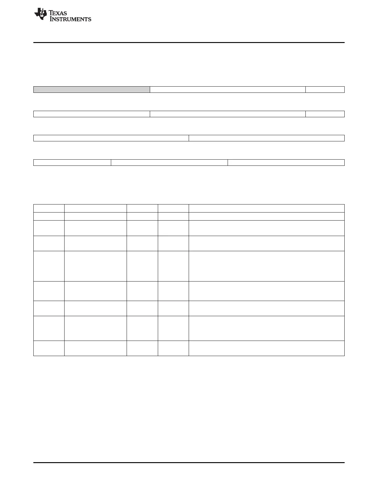
SDRAM_TIM_1 is shown in Figure 7-97 and described in Table 7-117.
Figure 7-97. SDRAM_TIM_1 Register
31 30 29 28 27 26 25 24
Reserved reg_t_rp reg_t_rcd
R-0h R/W-0h R/W-0h
23 22 21 20 19 18 17 16
reg_t_rcd reg_t_wr reg_t_ras
R/W-0h R/W-0h R/W-0h
15 14 13 12 11 10 9 8
reg_t_ras reg_t_rc
R/W-0h R/W-0h
7 6 5 4 3 2 1 0
reg_t_rc reg_t_rrd reg_t_wtr
R/W-0h R/W-0h R/W-0h
LEGEND: R/W = Read/Write; R = Read only; W1toCl = Write 1 to clear bit; -n = value after reset
Table 7-117. SDRAM_TIM_1 Register Field Descriptions
Bit Field Type Reset Description
31-29 Reserved R 0h
28-25 reg_t_rp R/W 0h
Minimum number of DDR clock cycles from Precharge to Activate or
Refresh, minus one.
24-21 reg_t_rcd R/W 0h
Minimum number of DDR clock cycles from Activate to Read or
Write, minus one.
20-17 reg_t_wr R/W 0h Minimum number of DDR clock cycles from last Write transfer to
Pre-charge, minus one.
The SDRAM initialization sequence will be started when the value of
this field is changed from the previous value and the EMIF is in
DDR2 mode.
16-12 reg_t_ras R/W 0h Minimum number of DDR clock cycles from Activate to Pre-charge,
minus one.
reg_t_ras >= reg_t_rcd.
11-6 reg_t_rc R/W 0h
Minimum number of DDR clock cycles from Activate to Activate,
minus one.
5-3 reg_t_rrd R/W 0h Minimum number of DDR clock cycles from Activate to Activate for a
different bank, minus one.
For an 8-bank DDR2 and DDR3, this field must be equal to
((tFAW/(4*tCK))-1).
2-0 reg_t_wtr R/W 0h
Minimum number of DDR clock cycles from last Write to Read,
minus one.
431
SPRUH73H–October 2011–Revised April 2013 Memory Subsystem
Submit Documentation Feedback
Copyright © 2011–2013, Texas Instruments Incorporated

 Loading...


