www.ti.com
GPMC
7.1.2.3 GPMC Signal List
The GPMC external interface signals are shown in Table 7-4.
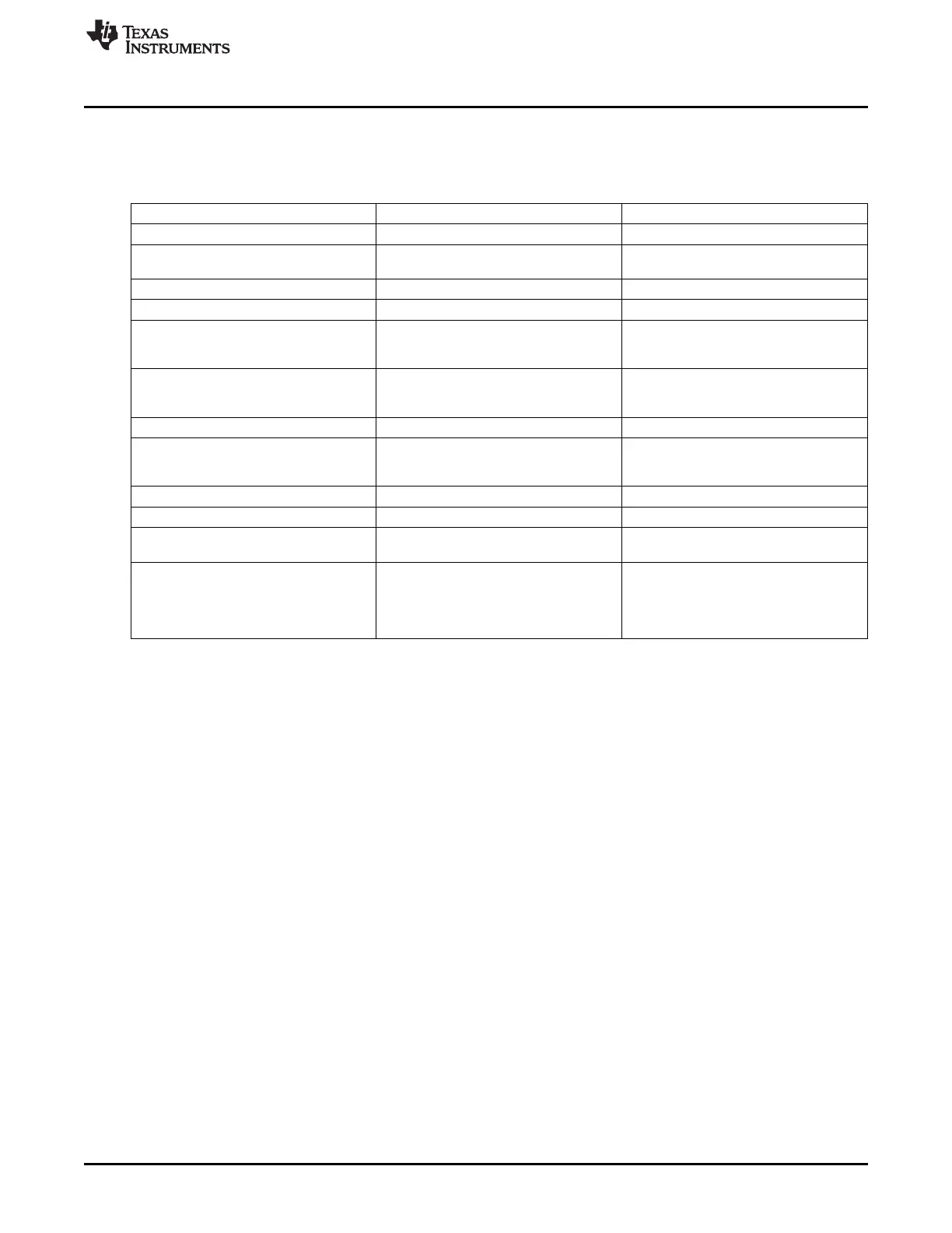
Table 7-4. GPMC Signal List
Signal Type Description
GPMC_A[27:0] O Address outputs
GPMC_AD[15:0] I/O Data - multiplexed with Address[16:1] and
Address[27:12]
GPMC_CSn[6:0] O Chip selects (active low)
GPMC_CLK O
(1)
Synchronous mode clock
GPMC_ADVn_ALE O Address Valid or Address Latch Enable
depending if NOR or NAND protocol
memories are selected.
GPMC_OEn_REn O Output Enable (active low). Also used as
Read Enable (active low) for NAND
protocol memories
GPMC_WEn O Write Enable (active low)
GPMC_BE0n_CLE O Lower Byte Enable (active low). Also used
as Command Latch Enable for NAND
protocol memories
GPMC_BE1n O Upper Byte Enable (active low)
GPMC_WPn O Write Protect (active low)
GPMC_WAIT[1:0] I External wait signal for NOR and NAND
protocol memories.
GPMC_DIR O GPMC.D[15:0] signal direction control
Low during transmit (for write access: data
OUT from GPMC to memory)
High during receive (for read access: data
IN from memory to GPMC)
(1)
GPMC_CLK is also used as a re-timing input. The associated CONF_<module>_<pin>_RXACTIVE bit for the output clock must
be set to 1 to enable the clock input back to the module. It is also recommended to place a 33-ohm resistor in series (close to
the processor) to avoid signal reflections.
255
SPRUH73H–October 2011–Revised April 2013 Memory Subsystem
Submit Documentation Feedback
Copyright © 2011–2013, Texas Instruments Incorporated

 Loading...


