LCD Registers
www.ti.com
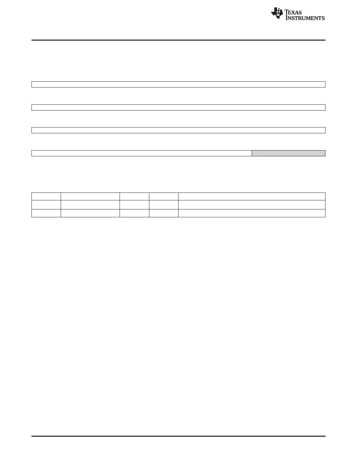
13.5.19 LCDDMA_FB1_BASE Register (offset = 4Ch) [reset = 0h]
LCDDMA_FB1_BASE is shown in Figure 13-37 and described in Table 13-32.
Figure 13-37. LCDDMA_FB1_BASE Register
31 30 29 28 27 26 25 24
fb1_base
R/W-0h
23 22 21 20 19 18 17 16
fb1_base
R/W-0h
15 14 13 12 11 10 9 8
fb1_base
R/W-0h
7 6 5 4 3 2 1 0
fb1_base Reserved
R/W-0h R-0h
LEGEND: R/W = Read/Write; R = Read only; W1toCl = Write 1 to clear bit; -n = value after reset
Table 13-32. LCDDMA_FB1_BASE Register Field Descriptions
Bit Field Type Reset Description
31-2 fb1_base R/W 0h
Frame Buffer 1 Base Address pointer
1-0 Reserved R 0h
1150
LCD Controller SPRUH73H–October 2011–Revised April 2013
Submit Documentation Feedback
Copyright © 2011–2013, Texas Instruments Incorporated

 Loading...


