www.ti.com
Functional Description
The one clock cycle is 20ns, which corresponds to 50-MHz frequency.
• Device detection
There is no specific identification routine executed prior to booting from an XIP device.
26.1.7.2.2 Pins Used
The list of device pins that are configured by the ROM in the case of NOR boot mode are as follows.
Please note that all the pins might not be driven at boot time. The decision as to which pins need to be
driven is done based on the type of NOR flash selected. The pins that are not listed below are not
configured by the ROM code and are left at power-on defaults. Specifically, external logic is needed to
isolate the upper address lines (A12–A27) of the NOR flash from the device pins and drive them low
during non-muxed NOR boot. Similarly for Muxed NOR Boot, address lines A16 and above to the memory
are not controlled by the ROM and need to be managed externally during boot to ensure proper
addressing to the all memory signals.
Once the initial software starts running, it can appropriately configure the pinmux setting for the lines and
remove the isolation to allow GPMC to drive all the address lines.
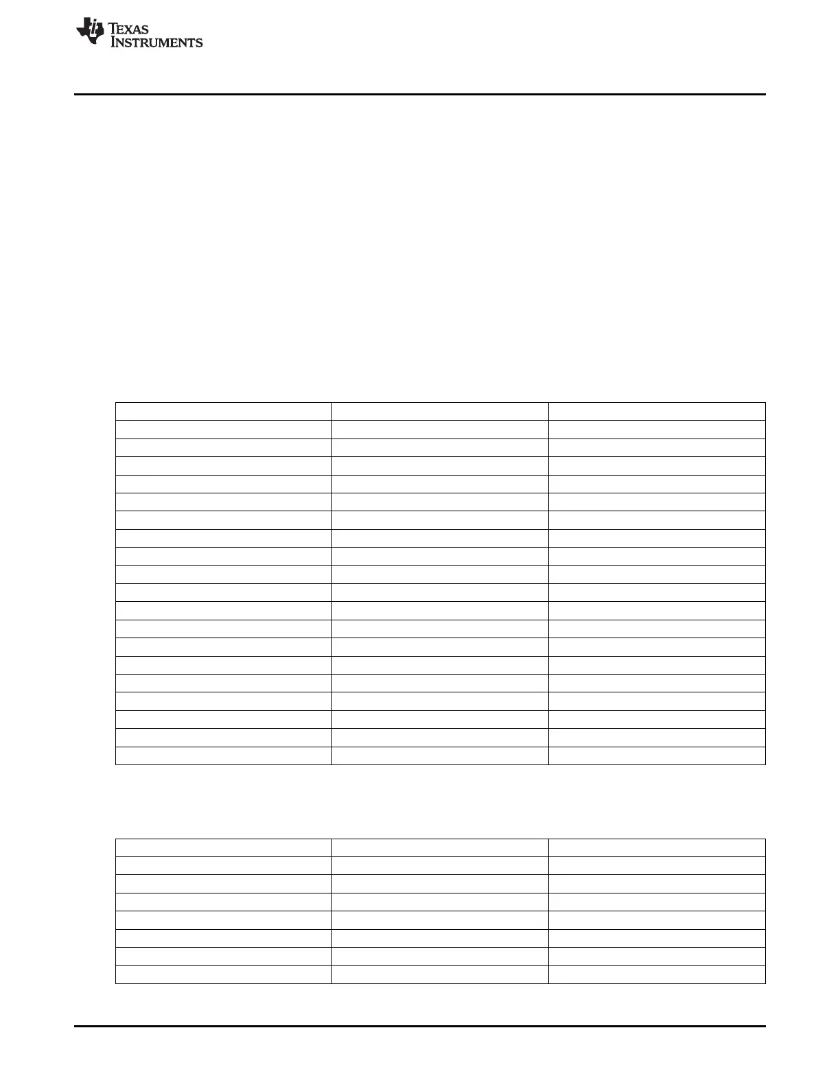
Table 26-9. Pins Used for Non-Muxed NOR Boot
Signal name Pin used in XIP_MUX1
(1)
mode Pin used in XIP_MUX2
(1)
mode
CS0 GPMC_CSN0 GPMC_CSN0
ADVN_ALE GPMC_ADVN_ALE GPMC_ADVN_ALE
OEN_REN GPMC_OEN_REN GPMC_OEN_REN
BE0N_CLE GPMC_BEN0_CLE GPMC_BEN0_CLE
WEN GPMC_WEN GPMC_WEN
WAIT GPMC_WAIT0 GPMC_WAIT0
AD0 - AD15 GPMC_AD0 - GPMC_AD15 GPMC_AD0 - GPMC_AD15
A0 GPMC_A0 LCD_DATA0
A1 GPMC_A1 LCD_DATA1
A2 GPMC_A2 LCD_DATA2
A3 GPMC_A3 LCD_DATA3
A4 GPMC_A4 LCD_DATA4
A5 GPMC_A5 LCD_DATA5
A6 GPMC_A6 LCD_DATA6
A7 GPMC_A7 LCD_DATA7
A8 GPMC_A8 LCD_VSYNC
A9 GPMC_A9 LCD_HSYNC
A10 GPMC_A10 LCD_PCLK
A11 GPMC_A11 LCD_AC_BIAS_EN
(1)
XIP_MUX1 and XIP_MUX2 do not correspond to the pin mux modes that are defined for each terminal. This table identifies
which pins are used in each boot mode.
Table 26-10. Pins Used for Muxed NOR Boot
Signal name Pin used in XIP_MUX1
(1)
mode Pin used in XIP_MUX2
(1)
mode
CS0 GPMC_CSN0 GPMC_CSN0
ADVN_ALE GPMC_ADVN_ALE GPMC_ADVN_ALE
OEN_REN GPMC_OEN_REN GPMC_OEN_REN
BE0N_CLE GPMC_BEN0_CLE GPMC_BEN0_CLE
WEN GPMC_WEN GPMC_WEN
WAIT GPMC_WAIT0 GPMC_WAIT0
AD0 - AD15 GPMC_AD0 - GPMC_AD15 GPMC_AD0 - GPMC_AD15
(1)
XIP_MUX1 and XIP_MUX2 do not correspond to the pin mux modes that are defined for each terminal. This table identifies
which pins are used in each boot mode.
4117
SPRUH73H–October 2011–Revised April 2013 Initialization
Submit Documentation Feedback
Copyright © 2011–2013, Texas Instruments Incorporated
 Loading...


