www.ti.com
LCD Registers
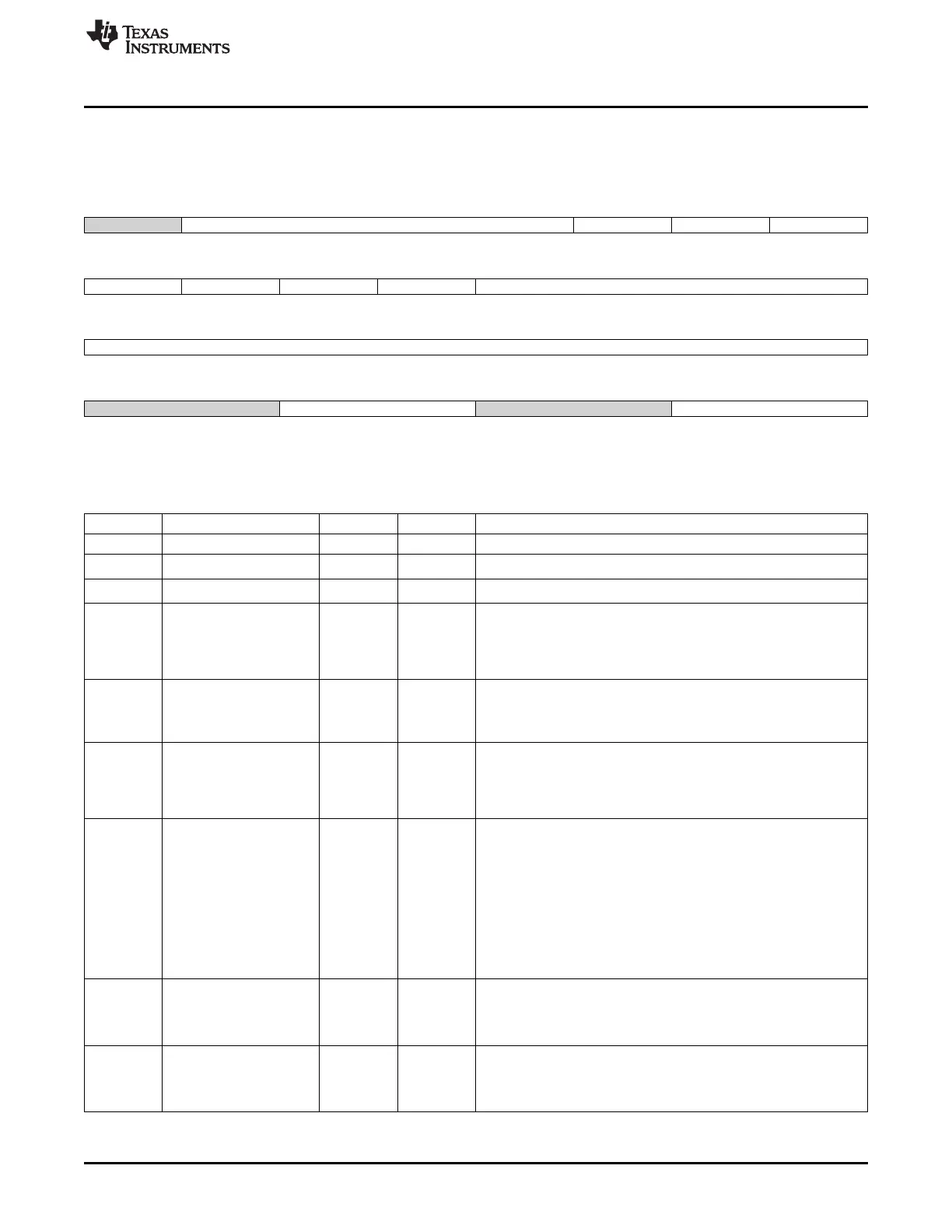
13.5.13 RASTER_TIMING_2 Register (offset = 34h) [reset = 0h]
RASTER_TIMING_2 is shown in Figure 13-31 and described in Table 13-26.
Figure 13-31. RASTER_TIMING_2 Register
31 30 29 28 27 26 25 24
Reserved hsw_highbits lpp_b10 phsvs_on_off phsvs_rf
R-0h R/W-0h R/W-0h R/W-0h R/W-0h
23 22 21 20 19 18 17 16
ieo ipc ihs ivs acbi
R/W-0h R/W-0h R/W-0h R/W-0h R/W-0h
15 14 13 12 11 10 9 8
acb
R/W-0h
7 6 5 4 3 2 1 0
Reserved hbp_highbits Reserved hfp_highbits
R-0h R/W-0h R-0h R/W-0h
LEGEND: R/W = Read/Write; R = Read only; W1toCl = Write 1 to clear bit; -n = value after reset
Table 13-26. RASTER_TIMING_2 Register Field Descriptions
Bit Field Type Reset Description
31 Reserved R 0h
30-27 hsw_highbits R/W 0h
Bits 9:6 of the horizontal sync width field
26 lpp_b10 R/W 0h
Lines Per Panel Bit 10 Bit 10 of the lpp field in RASTER_TIMING_1
25 phsvs_on_off R/W 0h Hsync/Vsync Pixel Clock Control On/Off 0 = lcd_lp and lcd_fp are
driven on opposite edges of pixel clock than the lcd_pixel_o 1 =
lcd_lp and lcd_fp are driven according to bit 24 Note that this bit
MUST be set to `0' for Passive Matrix displays
The edge timing is fixed
24 phsvs_rf R/W 0h Program HSYNC/VSYNC Rise or Fall 0: lcd_lp and lcd_fp are driven
on the rising edge of pixel clock (bit 25 must be set to 1)
1: lcd_lp and lcd_fp are driven on the falling edge of pixel clock (bit
25 must be set to 1)
23 ieo R/W 0h Invert Output Enable 0 = lcd_ac pin is active high in active display
mode 1 = lcd_ac pin is active low in active display mode Active
display mode: data driven out of the LCD's data lines on
programmed pixel clock edge where AC-bias is active
Note that ieo is ignored in passive display mode
22 ipc R/W 0h Invert Pixel Clock 0 = Data is driven on the LCD's data lines on the
rising edge of lcd_cp 1 = Data is driven on the LCD's data lines in
the falling edge of lcd_cp For Active Matrix output (cfg_lcdtft='1'), the
Output Pixel Clock is a free running clock in that it transitions in
horizontal blanking (including horizontal front porch, horizontal back
porch) areas and all vertical blanking times
For Passive Matrix output (cfg_lcdtft='0'), the Output Pixel Clock on
occurs when an output data value is written
It is in a return-to-zero state when cfg_ipc='0' and a return-to-one
state when cfg_ipc='1
'
21 ihs R/W 0h
Invert Hsync 0: lcd_lp pin is active high and inactive low 1: lcd_lp pin
is active low and inactive high Active and passive mode: horizontal
sync pulse/line clock active between lines, after the end of line wait
period
20 ivs R/W 0h
Invert Vsync 0 = lcd_fp pin is active high and inactive low 1 = lcd_fp
pin is active low and inactive high Active mode: vertical sync pulse
active between frames, after end of frame wait period Passive mode:
frame clock active during first line of each frame
1143
SPRUH73H–October 2011–Revised April 2013 LCD Controller
Submit Documentation Feedback
Copyright © 2011–2013, Texas Instruments Incorporated

 Loading...


