www.ti.com
CONTROL_MODULE Registers
9.3.89 ddr_cmd1_ioctrl Register (offset = 1408h) [reset = 0h]
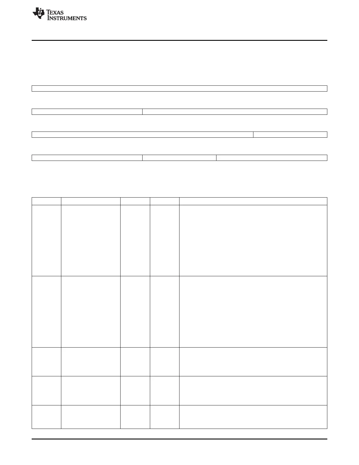
ddr_cmd1_ioctrl is shown in Figure 9-92 and described in Table 9-99.
Figure 9-92. ddr_cmd1_ioctrl Register
31 30 29 28 27 26 25 24
io_config_gp_wd1
R/W-0h
23 22 21 20 19 18 17 16
io_config_gp_wd1 io_config_gp_wd0
R/W-0h R/W-0h
15 14 13 12 11 10 9 8
io_config_gp_wd0 io_config_sr_clk
R/W-0h R/W-0h
7 6 5 4 3 2 1 0
io_config_i_clk io_config_sr io_config_i
R/W-0h R/W-0h R/W-0h
LEGEND: R/W = Read/Write; R = Read only; W1toCl = Write 1 to clear bit; -n = value after reset
Table 9-99. ddr_cmd1_ioctrl Register Field Descriptions
Bit Field Type Reset Description
31-21 io_config_gp_wd1 R/W 0h There are 2 bits per IO: io_config_gp_wd1 and io_config_gp_wd0.
For example:
macro pin 0: WD1 is bit 21, WD0 is bit 10
macro pin 1: WD1 is bit 22, WD0 is bit 11
...
macro pin 10: WD1 is bit 31, WD0 is bit 20
See the DDR PHY to IO Pin Mapping table in the Control Module
Functional Description section for a mapping of macro bits to I/Os.
WD1:WD0
00: Pullup/Pulldown disabled
01: Weak pullup enabled
10: Weak pulldown enabled
11: Weak keeper enabled
20-10 io_config_gp_wd0 R/W 0h There are 2 bits per IO: io_config_gp_wd1 and io_config_gp_wd0.
For example:
macro pin 0: WD1 is bit 21, WD0 is bit 10
macro pin 1: WD1 is bit 22, WD0 is bit 11
...
macro pin 10: WD1 is bit 31, WD0 is bit 20
See the DDR PHY to IO Pin Mapping table in the Control Module
Functional Description section for a mapping of macro bits to I/Os.
WD1:WD0
00: Pullup/Pulldown disabled
01: Weak pullup enabled
10: Weak pulldown enabled
11: Weak keeper enabled
9-8 io_config_sr_clk R/W 0h 2 bit to program clock IO Pads (DDR_CK/DDR_CKN) output slew
rate.
These connect as SR1, SR0 to the corresponding DDR IO buffer.
See the DDR Slew Rate Control Settings table in the Control Module
Functional Description section for a definition of these bits.
7-5 io_config_i_clk R/W 0h 3-bit configuration input to program clock IO pads
(DDR_CK/DDR_CKN) output impedance.
These connect as I2, I1, I0 to the corresponding DDR IO buffer.
See the DDR Impedance Control Settings table in the Control
Module Functional Description section for a definition of these bits.
4-3 io_config_sr R/W 0h 2 bit to program addr/cmd IO Pads output slew rate.
These connect as SR1, SR0 to the corresponding DDR IO buffer.
See the DDR Slew Rate Control Settings table in the Control Module
Functional Description section for a definition of these bits.
855
SPRUH73H–October 2011–Revised April 2013 Control Module
Submit Documentation Feedback
Copyright © 2011–2013, Texas Instruments Incorporated

 Loading...


