www.ti.com
USB Registers
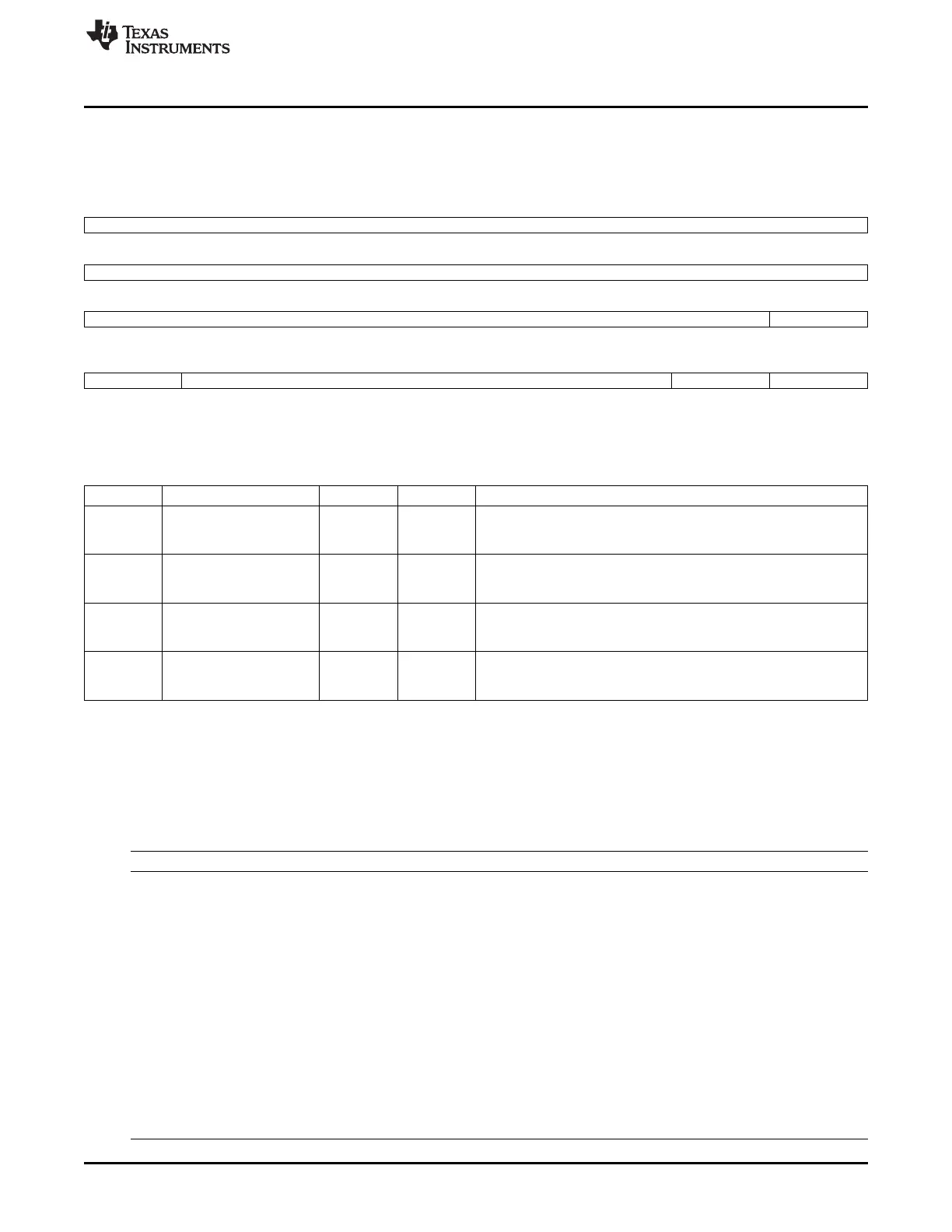
16.5.3.35 USB1MODE Register (offset = E8h) [reset = 100h]
USB1MODE is shown in Figure 16-133 and described in Table 16-143.
Figure 16-133. USB1MODE Register
31 30 29 28 27 26 25 24
Reserved
23 22 21 20 19 18 17 16
Reserved
15 14 13 12 11 10 9 8
Reserved IDDIG
R/W-1h
7 6 5 4 3 2 1 0
IDDIG_MUX Reserved PHY_TEST LOOPBACK
R/W-0h R/W-0h R/W-0h
LEGEND: R/W = Read/Write; R = Read only; W1toCl = Write 1 to clear bit; -n = value after reset
Table 16-143. USB1MODE Register Field Descriptions
Bit Field Type Reset Description
8 IDDIG R/W 1h MGC input value for iddig
0=A type
1=B type
7 IDDIG_MUX R/W 0h Multiplexer control for IDDIG signal going to the controller.
0 = IDDIG is from PHY1.
1 = IDDIG is from bit8 (IDDIG) of this USB1MODE register.
1 PHY_TEST R/W 0h PHY test
0 = Normal mode
1 = PHY test mode
0 LOOPBACK R/W 0h Loopback test mode
0 = Normal mode
1 = Loopback test mode USB1 Mode Register
16.5.4 USB2PHY Registers
Table 16-144 lists the memory-mapped registers for the USB2PHY. All register offset addresses not listed
in Table 16-144 should be considered as reserved locations and the register contents should not be
modified.
Table 16-144. USB2PHY REGISTERS
Offset Acronym Register Name Section
0h Termination_control Section 16.5.4.1
4h RX_CALIB Section 16.5.4.2
8h DLLHS_2 Section 16.5.4.3
Ch RX_TEST_2 Section 16.5.4.4
14h CHRG_DET Section 16.5.4.5
18h PWR_CNTL Section 16.5.4.6
1Ch UTMI_INTERFACE_CNTL_1 Section 16.5.4.7
20h UTMI_INTERFACE_CNTL_2 Section 16.5.4.8
24h BIST Section 16.5.4.9
28h BIST_CRC Section 16.5.4.10
2Ch CDR_BIST2 Section 16.5.4.11
30h GPIO Section 16.5.4.12
34h DLLHS Section 16.5.4.13
1901
SPRUH73H–October 2011–Revised April 2013 Universal Serial Bus (USB)
Submit Documentation Feedback
Copyright © 2011–2013, Texas Instruments Incorporated

 Loading...


