www.ti.com
Pulse-Width Modulation Subsystem (PWMSS)
15.1.2.2 PWMSS Clock and Reset Management
The PWMSS controllers have separate bus interface and functional clocks.
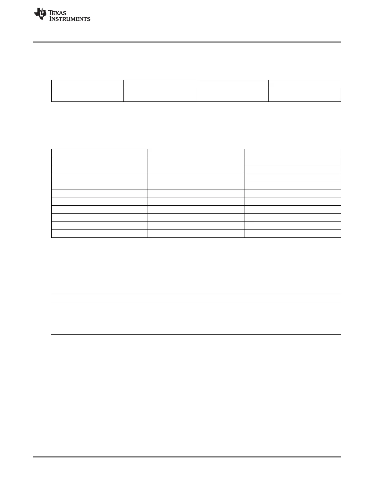
Table 15-3. PWMSS Clock Signals
Clock Signal Max Freq Reference / Source Comments
PWMSS_ocp_clk 100 MHz CORE_CLKOUTM4 / 2 pd_per_l4ls_gclk
Interface / Functional clock from PRCM
15.1.2.3 PWMSS Pin list
The external signals for the PWMSS module are shown in the following table.
Table 15-4. PWMSS Pin List
Pin Type* Description
EPWMxA O PWM output A
EPWMxB O PWM output B
EPWM_SYNCIN I PWM Sync input
EPWM_SYNCOUT O PWM Sync output
EPWM_TRIPZONE[5:0] I PWM Tripzone inputs
ECAP_CAPIN_APWMOUT I/O eCAP Capture input / PWM output
EQEP_A I/O eQEP Quadrature input/output
EQEP_B I/O eQEP Quadrature input/output
EQEP_INDEX I/O eQEP Index input/output
EQEP_STROBE I/O eQEP Strobe input/output
15.1.3 PWMSS Registers
Table 15-5 lists the memory-mapped registers for the PWMSS. All register offset addresses not listed in
Table 15-5 should be considered as reserved locations and the register contents should not be modified.
Table 15-5. PWMSS REGISTERS
Offset Acronym Register Name Section
0h IDVER IP Revision Register Section 15.1.3.1
4h SYSCONFIG System Configuration Register Section 15.1.3.2
8h CLKCONFIG Clock Configuration Register Section 15.1.3.3
Ch CLKSTATUS Clock Status Register Section 15.1.3.4
1489
SPRUH73H–October 2011–Revised April 2013 Pulse-Width Modulation Subsystem (PWMSS)
Submit Documentation Feedback
Copyright © 2011–2013, Texas Instruments Incorporated

 Loading...


