www.ti.com
GPMC
7.1.5.12 GPMC_CONFIG2_i
Chip-select signal timing parameter configuration.
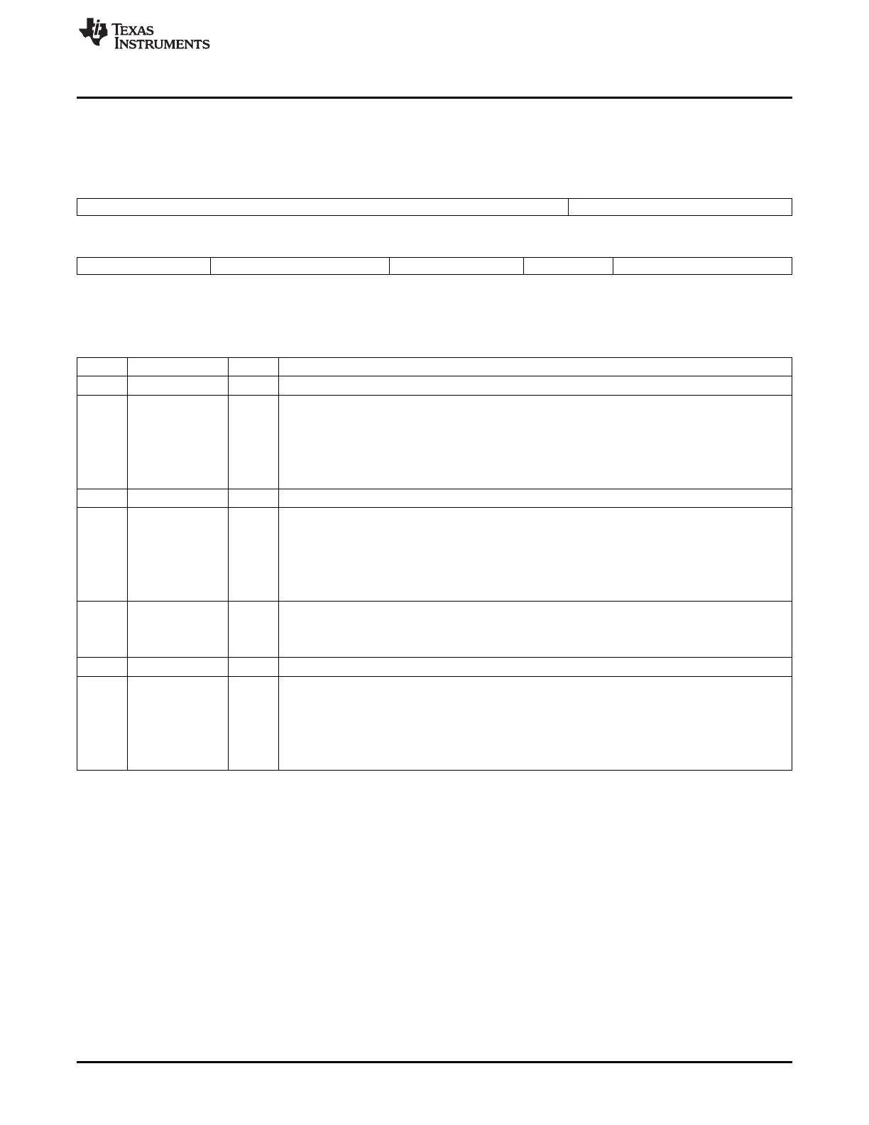
Figure 7-62. GPMC_CONFIG2_i
31 21 20 16
Reserved CSWROFFTIME
R-0 R/W-0
15 13 12 8 7 6 4 3 0
Reserved CSRDOFFTIME CSEXTRADELAY Reserved CSONTIME
R-0 R/W-0 R/W-0 R-0 R/W-0
LEGEND: R/W = Read/Write; R = Read only; -n = value after reset
Table 7-66. GPMC_CONFIG2_i Field Descriptions
Bit Field Value Description
31-21 Reserved 0 Reserved
20-16 CSWROFFTIME CS# de-assertion time from start cycle time for write accesses
0 0 GPMC_FCLK cycle
1h 1 GPMC_FCLK cycle
⋮ ⋮
1Fh 31 GPMC_FCLK cycles
15-13 Reserved 0 Reserved
12-8 CSRDOFFTIME CS# de-assertion time from start cycle time for read accesses
0 0 GPMC_FCLK cycle
1h 1 GPMC_FCLK cycle
⋮ ⋮
1Fh 31 GPMC_FCLK cycles
7 CSEXTRADELAY CS# Add Extra Half GPMC.FCLK cycle
0 CS i Timing control signal is not delayed
1 CS i Timing control signal is delayed of half GPMC_FCLK clock cycle
6-4 Reserved 0 Reserved
3-0 CSONTIME CS# assertion time from start cycle time
0 0 GPMC_FCLK cycle
1h 1 GPMC_FCLK cycle
⋮ ⋮
1Fh 15 GPMC_FCLK cycles
377
SPRUH73H–October 2011–Revised April 2013 Memory Subsystem
Submit Documentation Feedback
Copyright © 2011–2013, Texas Instruments Incorporated

 Loading...


