Multimedia Card Registers
www.ti.com
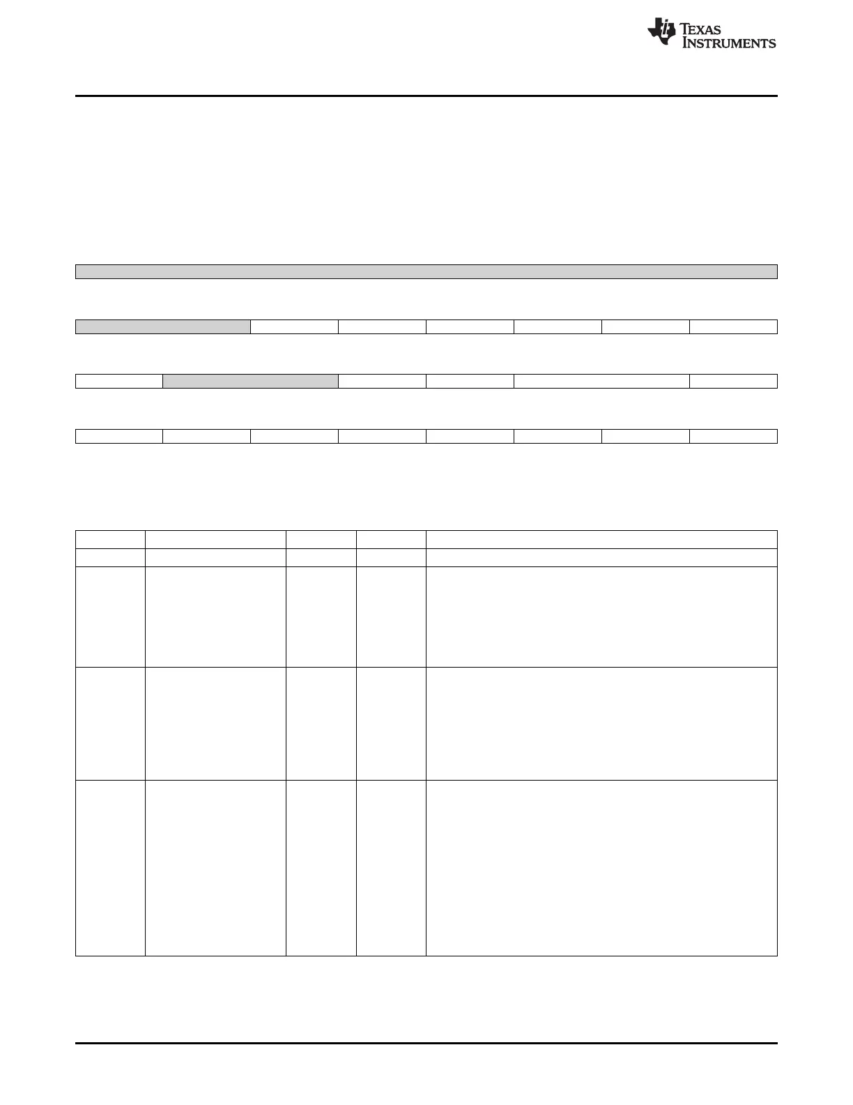
18.5.1.5 SD_CON Register (offset = 12Ch) [reset = 0h]
SD_CON is shown in Figure 18-41 and described in Table 18-24.
This register is used: To select the functional mode for any card. To send an initialization sequence to any
card. To send an initialization sequence to any card. To enable the detection on the mmc_dat[1] signal of
a card interrupt for SDIO cards only. It also configures the parameters related to the card detect and write
protect input signals
Figure 18-41. SD_CON Register
31 30 29 28 27 26 25 24
Reserved
R-0h
23 22 21 20 19 18 17 16
Reserved SDMA_LnE DMA_MnS DDR BOOT_CF0 BOOT_ACK CLKEXTFREE
R-0h R/W-0h R/W-0h R/W-0h R/W-0h R/W-0h R/W-0h
15 14 13 12 11 10 9 8
PADEN Reserved CEATA CTPL DVAL WPP
R/W-0h R-0h R/W-0h R/W-0h R/W-0h R/W-0h
7 6 5 4 3 2 1 0
CDP MIT DW8 MODE STR HR INIT OD
R/W-0h R/W-0h R/W-0h R/W-0h R/W-0h R/W-0h R/W-0h R/W-0h
LEGEND: R/W = Read/Write; R = Read only; W1toCl = Write 1 to clear bit; -n = value after reset
Table 18-24. SD_CON Register Field Descriptions
Bit Field Type Reset Description
31-22 Reserved R 0h
21 SDMA_LnE R/W 0h Slave DMA Level/Edge Request.
The waveform of the DMA request can be configured either edge
sensitive with early de-assertion on first access to SD_DATA register
or late de-assertion, request remains active until last allowed data
written into SD_DATA.
0x0 = Slave DMA edge sensitive.
0x1 = Slave DMA level sensitive.
20 DMA_MnS R/W 0h DMA Master or Slave selection.
When this bit is set and the controller is configured to use the DMA,
Ocp master interface is used to get datas from system using ADMA2
procedure (direct access to the memory).
This option is only available if generic parameter MADMA_EN is
asserted to 1.
0x0 = The controller is slave on data transfers with system.
0x1 = Not available on this device.
19 DDR R/W 0h Dual Data Rate mode.
When this register is set, the controller uses both clock edge to emit
or receive data.
Odd bytes are transmitted on falling edges and even bytes are
transmitted on rise edges.
It only applies on Data bytes and CRC, Start, end bits and CRC
status are kept full cycle.
This bit field is only meaningful and active for even clock divider ratio
of SD_SYSCTL[CLKD], it is insensitive to SD_HCTL[HSPE] setting.
Note: DDR mode is not supported on AM335x.
Always set this bit to 0.
0x0 = Standard modeData are transmitted on a single edge.
0x1 = Data Bytes and CRC are transmitted on both edges.
3398
Multimedia Card (MMC) SPRUH73H–October 2011–Revised April 2013
Submit Documentation Feedback
Copyright © 2011–2013, Texas Instruments Incorporated

 Loading...


