CONTROL_MODULE Registers
www.ti.com
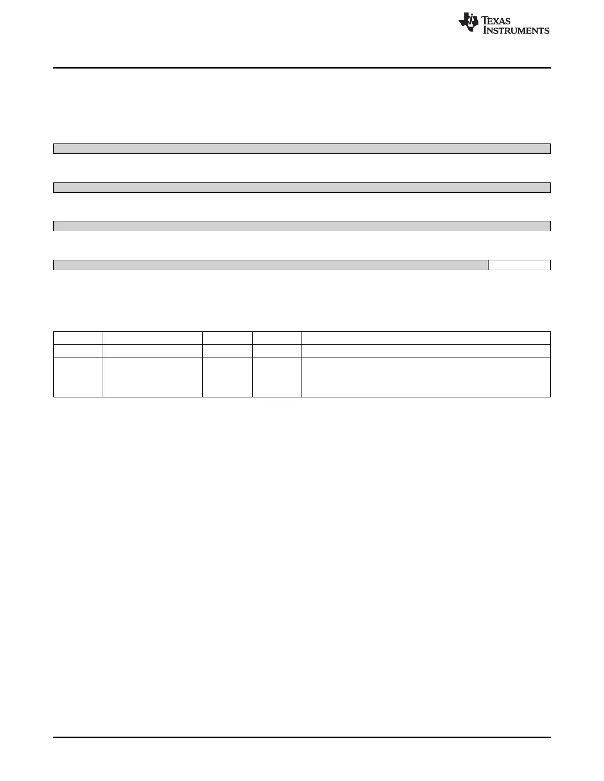
9.3.77 ddr_cke_ctrl Register (offset = 131Ch) [reset = 0h]
ddr_cke_ctrl is shown in Figure 9-80 and described in Table 9-87.
Figure 9-80. ddr_cke_ctrl Register
31 30 29 28 27 26 25 24
Reserved
R-0h
23 22 21 20 19 18 17 16
Reserved
R-0h
15 14 13 12 11 10 9 8
Reserved
R-0h
7 6 5 4 3 2 1 0
Reserved ddr_cke_ctrl
R-0h R/W-0h
LEGEND: R/W = Read/Write; R = Read only; W1toCl = Write 1 to clear bit; -n = value after reset
Table 9-87. ddr_cke_ctrl Register Field Descriptions
Bit Field Type Reset Description
31-1 Reserved R 0h
0 ddr_cke_ctrl R/W 0h CKE from EMIF/DDRPHY is ANDed with this bit.
0: CKE to memories gated off to zero. External DRAM memories will
not able to register DDR commands from device
1: Normal operation. CKE is now controlled by EMIF/DDR PHY.
842
Control Module SPRUH73H–October 2011–Revised April 2013
Submit Documentation Feedback
Copyright © 2011–2013, Texas Instruments Incorporated

 Loading...


