www.ti.com
USB Registers
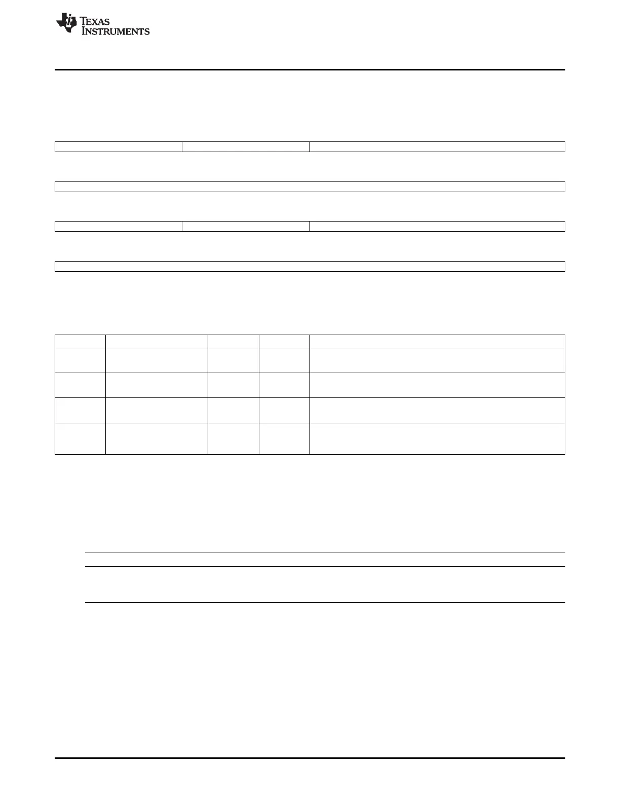
16.5.5.123 RXHPCRB29 Register (offset = BB0h) [reset = 0h]
RXHPCRB29 is shown in Figure 16-274 and described in Table 16-286.
Figure 16-274. RXHPCRB29 Register
31 30 29 28 27 26 25 24
Reserved RX_HOST_FDQ3_QMGR RX_HOST_FDQ3_QNUM
W-0h W-0h
23 22 21 20 19 18 17 16
RX_HOST_FDQ3_QNUM
W-0h
15 14 13 12 11 10 9 8
Reserved RX_HOST_FDQ2_QMGR RX_HOST_FDQ2_QNUM
W-0h W-0h
7 6 5 4 3 2 1 0
RX_HOST_FDQ2_QNUM
W-0h
LEGEND: R/W = Read/Write; R = Read only; W1toCl = Write 1 to clear bit; -n = value after reset
Table 16-286. RXHPCRB29 Register Field Descriptions
Bit Field Type Reset Description
29-28 RX_HOST_FDQ3_QMGR W 0h
This field specifies which Manager should be used for the 4th or later
Rx buffers in a host type packet
27-16 RX_HOST_FDQ3_QNUM W 0h
This field specifies which Free Descriptor Queue should be used for
the 4th or later Rx buffers in a host type packet
13-12 RX_HOST_FDQ2_QMGR W 0h
This field specifies which Buffer Manager should be used for the 3rd
Rx buffer in a host type packet
11-0 RX_HOST_FDQ2_QNUM W 0h This field specifies which Free Descriptor / Buffer Pool should be
used for the 3rd Rx buffer in a host type packet Table
101 -Rx Channel N Host Packet Configuration Registers B
16.5.6 CPPI_DMA_SCHEDULER Registers
Table 16-287 lists the memory-mapped registers for the CPPI_DMA_SCHEDULER. All register offset
addresses not listed in Table 16-287 should be considered as reserved locations and the register contents
should not be modified.
Table 16-287. CPPI_DMA_SCHEDULER REGISTERS
Offset Acronym Register Name Section
0h DMA_SCHED_CTRL Section 16.5.6.1
800h to WORD0 to WORD63 Section 16.5.6.2
900h
2081
SPRUH73H–October 2011–Revised April 2013 Universal Serial Bus (USB)
Submit Documentation Feedback
Copyright © 2011–2013, Texas Instruments Incorporated

 Loading...


