McASP Registers
www.ti.com
22.4.1.29 Transmit Clock Control Register (ACLKXCTL)
The transmit clock control register (ACLKXCTL) configures the transmit bit clock (ACLKX) and the transmit
clock generator. The ACLKXCTL is shown in Figure 22-67 and described in Table 22-40.
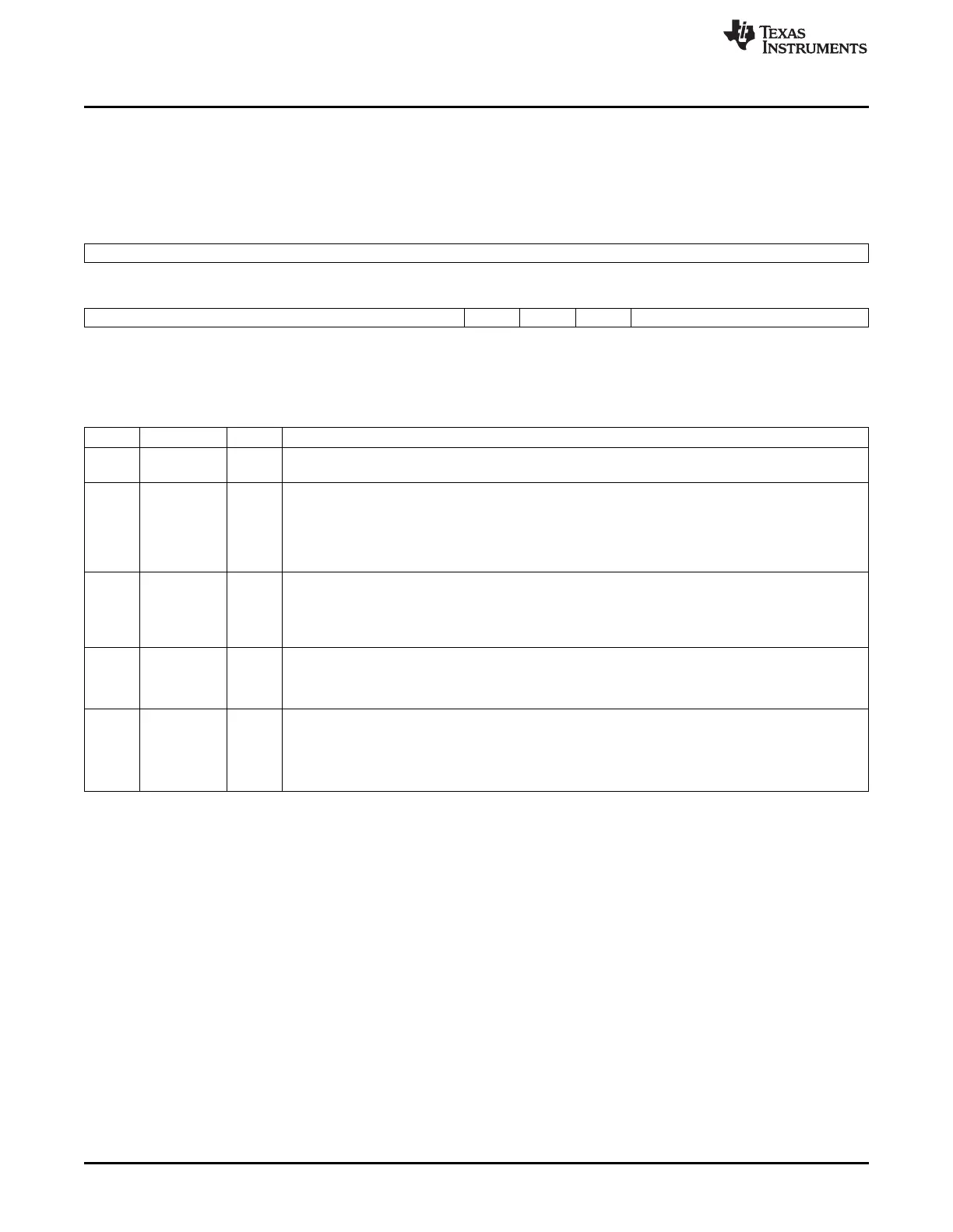
Figure 22-67. Transmit Clock Control Register (ACLKXCTL)
31 16
Reserved
R-0
15 8 7 6 5 4 0
Reserved CLKXP ASYNC CLKXM CLKXDIV
R-0 R/W-0 R/W-1 R/W-1 R/W-0
LEGEND: R/W = Read/Write; R = Read only; -n = value after reset
Table 22-40. Transmit Clock Control Register (ACLKXCTL) Field Descriptions
Bit Field Value Description
31-8 Reserved 0 Reserved. The reserved bit location always returns the default value. A value written to this field has no
effect. If writing to this field, always write the default value for future device compatibility.
7 CLKXP Transmit bitstream clock polarity select bit.
0 Rising edge. External receiver samples data on the falling edge of the serial clock, so the transmitter
must shift data out on the rising edge of the serial clock.
1 Falling edge. External receiver samples data on the rising edge of the serial clock, so the transmitter
must shift data out on the falling edge of the serial clock.
6 ASYNC Transmit/receive operation asynchronous enable bit.
0 Synchronous. Transmit clock and frame sync provides the source for both the transmit and receive
sections.
1 Asynchronous. Separate clock and frame sync used by transmit and receive sections.
5 CLKXM Transmit bit clock source bit.
0 External transmit clock source from ACLKX pin.
1 Internal transmit clock source from output of programmable bit clock divider.
4-0 CLKXDIV 0-1Fh Transmit bit clock divide ratio bits determine the divide-down ratio from AHCLKX to ACLKX.
0 Divide-by-1.
1h Divide-by-2.
2h-1Fh Divide-by-3 to divide-by-32.
3866
Multichannel Audio Serial Port (McASP) SPRUH73H–October 2011–Revised April 2013
Submit Documentation Feedback
Copyright © 2011–2013, Texas Instruments Incorporated

 Loading...


