OCMC0
L3_FAST
Interconnect
RAM Bank
(64K Total)
Control
Module
www.ti.com
OCMC-RAM
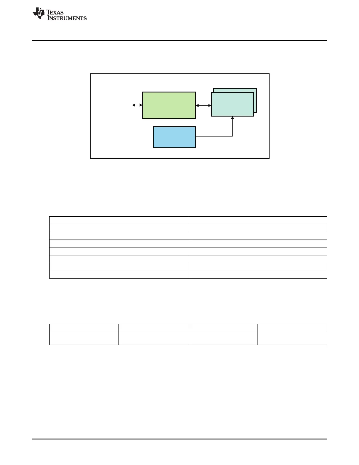
7.2.2 Integration
This device includes a single instantiation of the on-chip memory controller interfacing to a single 64K
bank of RAM.
Figure 7-87. OCMC RAM Integration
7.2.2.1 OCMC RAM Connectivity Attributes
The general connectivity attributes for the OCMC RAM modules are summarized in Table 7-91.
Table 7-91. OCMC RAM Connectivity Attributes
Attributes Type
Power Domain Peripheral Domain
Clock Domain PD_PER_L3_GCLK
Reset Signals PER_DOM_RST_N
Idle/Wakeup Signals Smart Idle
Interrupt Requests None
DMA Requests None
Physical Address L3 Fast slave port
7.2.2.2 OCMC RAM Clock and Reset Management
The OCMC module uses a single clock for the module and its OCP interface.
Table 7-92. OCMC RAM Clock Signals
Clock Signal Max Freq Reference / Source Comments
prcm_ocmc_clock 200 MHz CORE_CLKOUTM4 pd_per_l3_gclk
Interface / Functional clock From PRCM
7.2.2.3 OCMC RAM Pin List
The OCMC RAM module does not include any external interface pins.
399
SPRUH73H–October 2011–Revised April 2013 Memory Subsystem
Submit Documentation Feedback
Copyright © 2011–2013, Texas Instruments Incorporated

 Loading...


