www.ti.com
Integration
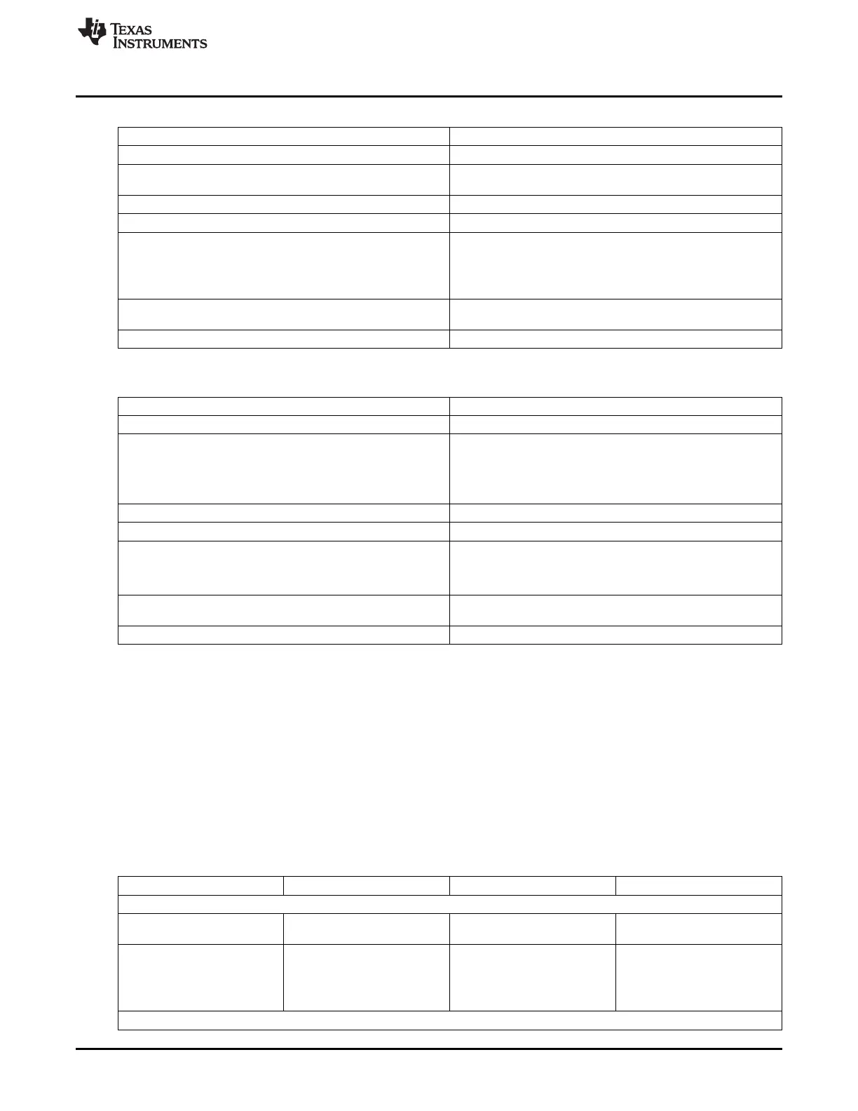
Table 25-1. GPIO0 Connectivity Attributes
Attributes Type
Power Domain Wakeup Domain
Clock Domain PD_WKUP_L4_WKUP_GCLK (OCP)
GPIO_0_GDBCLK (Debounce)
Reset Signals WKUP_DOM_RST_N
Idle/Wakeup Signals Smart Idle / Slave Wakeup
Interrupt Requests
Two Interrupts:
INTRPEND1 (GPIOINT0A) to MPU subsystem, PRU-ICSS
(POINTRPEND1), and WakeM3
INTRPEND2 (GPIOINT0B) to MPU subsystem and WakeM3
DMA Requests Interrupt Requests are redirected as DMA requests: 1 DMA
request (GPIOEVT0)
Physical Address L4 Wakeup slave port
Table 25-2. GPIO[1:3] Connectivity Attributes
Attributes Type
Power Domain Peripheral Domain
Clock Domain
PD_PER_L4LS_GCLK (OCP)
GPIO_1_GDBCLK (GPIO1 Debounce)
GPIO_2_GDBCLK (GPIO2 Debounce)
GPIO_3_GDBCLK (GPIO3 Debounce)
Reset Signals PER_DOM_RST_N
Idle/Wakeup Signals Smart Idle
Interrupt Requests
Two Interrupts:
INTRPEND1 (GPIOINTxA) to MPU subsystem
INTRPEND2 (GPIOINTxB) to MPU subsystem
DMA Requests Interrupt Requests are redirected as DMA requests: 1 DMA
request only for GPIO1 (GPIOEVT1) and GPIO2 (GPIOEVT2)
Physical Address L4 Peripheral slave port
25.2.2 GPIO Clock and Reset Management
The GPIO modules require two clocks: The de-bounce clock is used for the de-bouncing cells. The
interface clock provided by the peripheral bus (L4 interface) is also the functional clock and is used
through the entire GPIO module (except within the de-bouncing sub-module). It clocks the OCP interface
and the internal logic. For GPIO0 the debounce clock is selected from one of three sources using the
CLKSEL_GPIO0_DBCLK register in the PRCM:
• The on-chip ~32.768 KHz oscillator (CLK_RC32K)
• The PER PLL generated 32.768 KHz clock (CLK_32KHZ)
• The external 32.768 KHz oscillator/clock (CLK_32K_RTC)
Table 25-3. GPIO Clock Signals
Clock Signal Max Freq Reference / Source Comments
GPIO0
Functional / Interface clock 100 MHz CORE_CLKOUTM4 / 2 pd_wkup_l4_wkup_gclk
From PRCM
Debounce Functional clock 32.768 KHz pd_wkup_gpio0_gdbclk
CLK_RC32K
From PRCM
CLK_32KHZ
(PER_CLKOUTM2 / 5859.375)
CLK_32K_RTC
GPIO[1:3]
4059
SPRUH73H–October 2011–Revised April 2013 General-Purpose Input/Output
Submit Documentation Feedback
Copyright © 2011–2013, Texas Instruments Incorporated

 Loading...


