www.ti.com
USB Registers
16.5.4.18 ANA_CONFIG2 Register (offset = 54h) [reset = 0h]
ANA_CONFIG2 is shown in Figure 16-151 and described in Table 16-162.
Used to configure and debug the analog blocks.
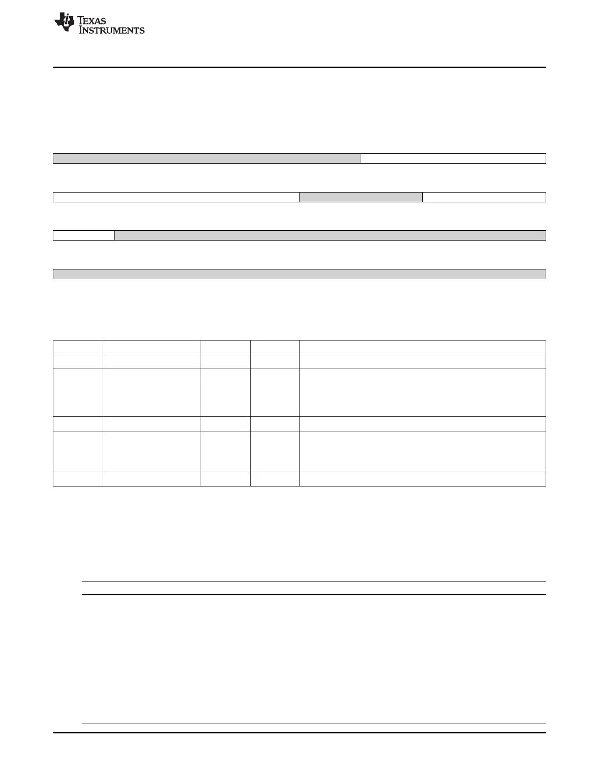
Figure 16-151. ANA_CONFIG2 Register
31 30 29 28 27 26 25 24
Reserved REF_GEN_TEST
R-0h R/W-0h
23 22 21 20 19 18 17 16
REF_GEN_TEST Reserved RTERM_TEST
R/W-0h R/W-0h R/W-0h
15 14 13 12 11 10 9 8
RTERM_TEST Reserved
R/W-0h R/W-0h
7 6 5 4 3 2 1 0
Reserved
R/W-0h
LEGEND: R/W = Read/Write; R = Read only; W1toCl = Write 1 to clear bit; -n = value after reset
Table 16-162. ANA_CONFIG2 Register Field Descriptions
Bit Field Type Reset Description
31-27 Reserved R 0h
Reserved.
26-20 REF_GEN_TEST R/W 0h 0000000b - Produces the typical vertical eye diagram amplitude
(default).
1100000b - Increases vertical eye diagram amplitude by 15 mV.
1010000b - Decreases vertical eye diagram amplitude by 15 mV.
All other values are reserved.
19-18 Reserved R/W 0h
Reserved.
17-15 RTERM_TEST R/W 0h 000b - Typical termination impedance (default).
011b - Decreases the termination impedance by 2 to 3% and can be
used to increase the vertical eye diagram amplitude by 1 to 1.5%.
All other values reserved.
14-0 Reserved R/W 0h
Reserved.
16.5.5 CPPI_DMA Registers
Table 16-163 lists the memory-mapped registers for the CPPI_DMA. All register offset addresses not
listed in Table 16-163 should be considered as reserved locations and the register contents should not be
modified.
Table 16-163. CPPI_DMA REGISTERS
Offset Acronym Register Name Section
0h DMAREVID Section 16.5.5.1
4h TDFDQ Section 16.5.5.2
8h DMAEMU Section 16.5.5.3
800h TXGCR0 Section 16.5.5.4
808h RXGCR0 Section 16.5.5.5
80Ch RXHPCRA0 Section 16.5.5.6
810h RXHPCRB0 Section 16.5.5.7
820h TXGCR1 Section 16.5.5.8
828h RXGCR1 Section 16.5.5.9
82Ch RXHPCRA1 Section 16.5.5.10
1925
SPRUH73H–October 2011–Revised April 2013 Universal Serial Bus (USB)
Submit Documentation Feedback
Copyright © 2011–2013, Texas Instruments Incorporated

 Loading...


