www.ti.com
GPMC
7.1.5.16 GPMC_CONFIG6_i
WrAccessTime, WrDataOnADmuxBus, Cycle2Cycle, and BusTurnAround parameters configuration
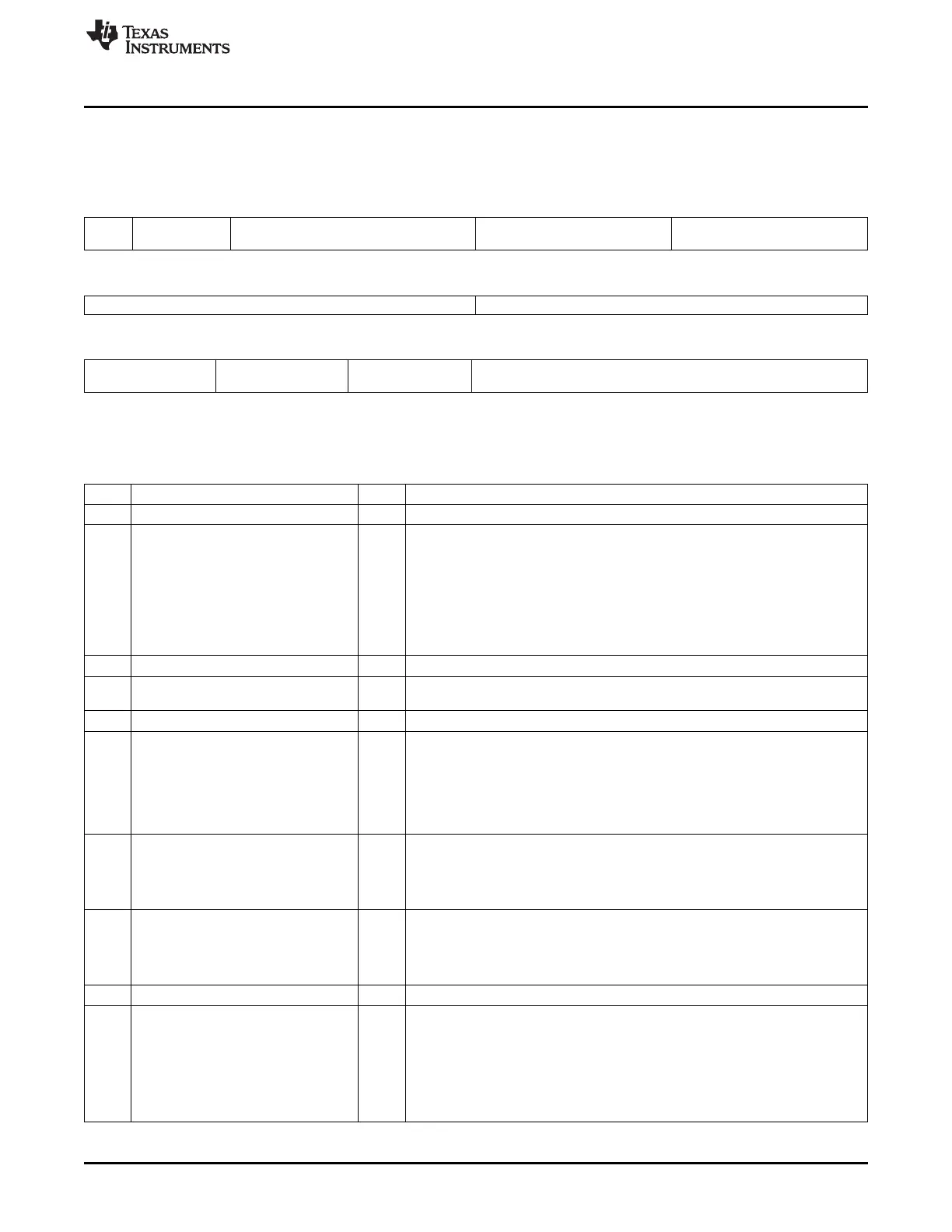
Figure 7-66. GPMC_CONFIG6_i
31 30 29 28 24 23 20 19 16
Reserv Reserved WRACCESSTIME Reserved WRDATAONADMUXBUS
ed
R-1 R-0 R/W-F R-0 R/W-7
15 12 11 8
Reserved CYCLE2CYCLEDELAY
R-0 R/W-0
7 6 5 4 3 0
CYCLE2CYCLE CYCLE2CYCLE Reserved BUSTURNAROUND
SAMECSEN DIFFCSEN
R/W-0 R/W-0 R-0 R/W-0
LEGEND: R/W = Read/Write; R = Read only; -n = value after reset
Table 7-70. GPMC_CONFIG6_i Field Descriptions
Bit Field Value Description
31-29 Reserved 1 Reserved
28-24 WRACCESSTIME Delay from StartAccessTime to the GPMC.FCLK rising edge corresponding the
the GPMC.CLK rising edge used by the attached memory for the first data
capture
0 0 GPMC_FCLK cycle
1h 1 GPMC_FCLK cycle
⋮ ⋮
1Fh 31 GPMC_FCLK cycles
23-20 Reserved 0 Reserved
19-16 WRDATAONADMUXBUS 0-Fh Specifies on which GPMC.FCLK rising edge the first data of the synchronous
burst write is driven in the add/data multiplexed bus
15-12 Reserved 0 Reserved
11-8 CYCLE2CYCLEDELAY Chip select high pulse delay between two successive accesses
0 0 GPMC_FCLK cycle
1h 1 GPMC_FCLK cycle
⋮ ⋮
Fh 15 GPMC_FCLK cycles
7 CYCLE2CYCLESAMECSEN Add Cycle2CycleDelay between two successive accesses to the same chip-
select (any access type)
0 No delay between the two accesses
1 Add CYCLE2CYCLEDELAY
6 CYCLE2CYCLEDIFFCSEN Add Cycle2CycleDelay between two successive accesses to a different chip-
select (any access type)
0 No delay between the two accesses
1 Add CYCLE2CYCLEDELAY
5-4 Reserved 0 Reserved
3-0 BUSTURNAROUND Bus turn around latency between two successive accesses to the same chip-
select (read to write) or to a different chip-select (read to read and read to write)
0 0 GPMC_FCLK cycle
1h 1 GPMC_FCLK cycle
⋮ ⋮
Fh 15 GPMC_FCLK cycles
383
SPRUH73H–October 2011–Revised April 2013 Memory Subsystem
Submit Documentation Feedback
Copyright © 2011–2013, Texas Instruments Incorporated

 Loading...


