www.ti.com
USB Registers
16.5.7.13 LRAM1BASE Register (offset = 88h) [reset = 0h]
LRAM1BASE is shown in Figure 16-289 and described in Table 16-303.
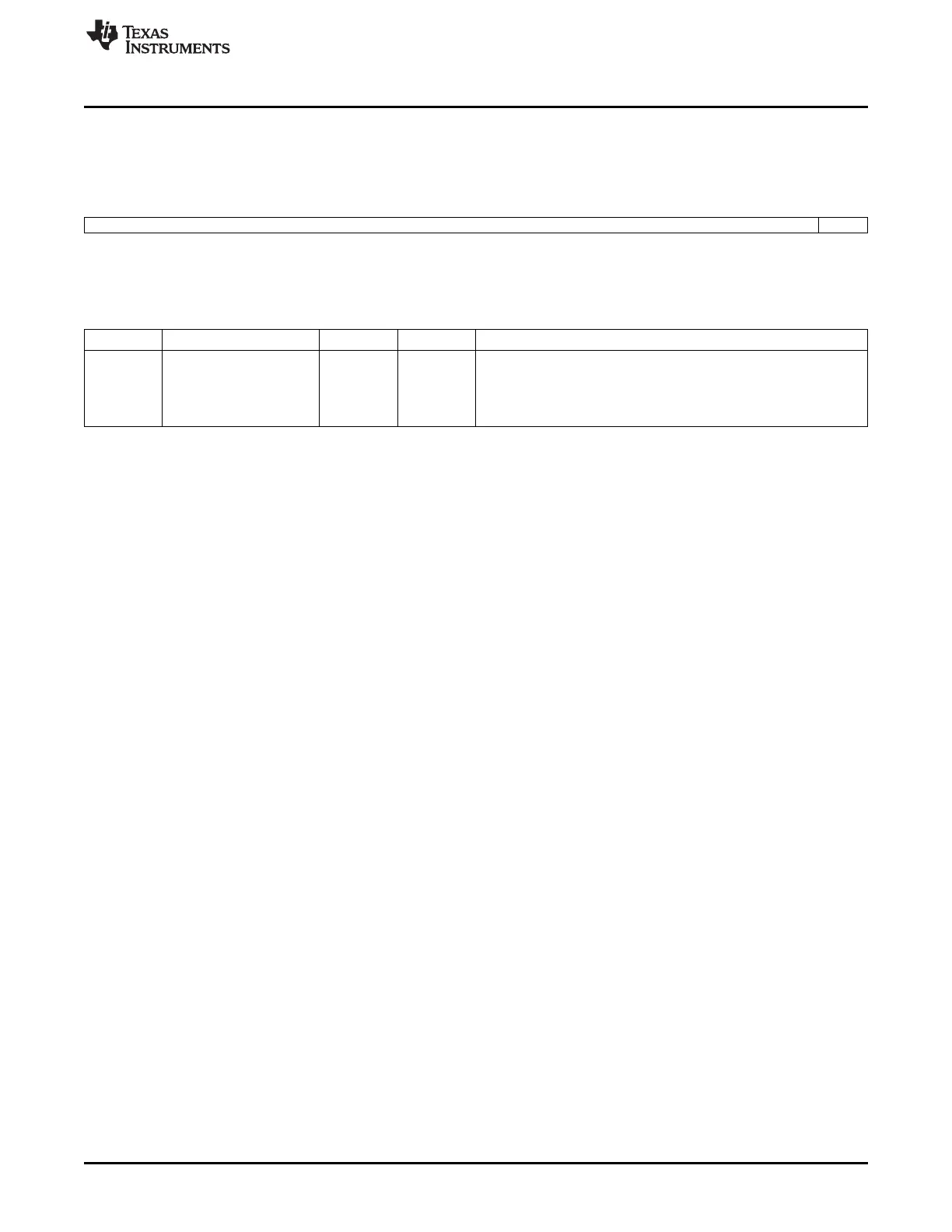
Figure 16-289. LRAM1BASE Register
31 30 29 28 27 26 25 24 23 22 21 20 19 18 17 16 15 14 13 12 11 10 9 8 7 6 5 4 3 2 1 0
REGION1_BASE Reserved
R/W-0
LEGEND: R/W = Read/Write; R = Read only; W1toCl = Write 1 to clear bit; -n = value after reset
Table 16-303. LRAM1BASE Register Field Descriptions
Bit Field Type Reset Description
31-2 REGION1_BASE R/W-0 0 This field stores the base address for the second region of the
linking RAM.
This may be anywhere in
32- bit address space but would be typically located in off- chip
memory.
2121
SPRUH73H–October 2011–Revised April 2013 Universal Serial Bus (USB)
Submit Documentation Feedback
Copyright © 2011–2013, Texas Instruments Incorporated

 Loading...


