www.ti.com
Integration
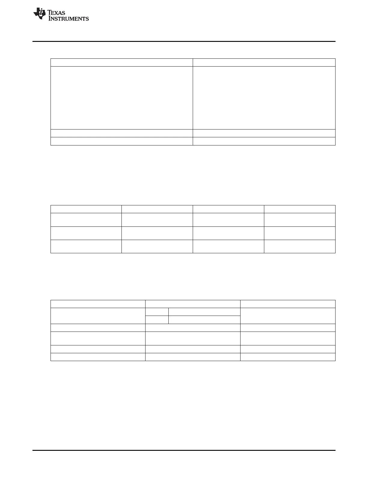
Table 16-1. USB Connectivity Attributes (continued)
Attributes Type
Interrupt request
4 interrupts
usbss (USBSSINT) to MPU subsystem
usb0 (USBINT0) to MPU subsystem
usb1 (USBINT1) to MPU subsystem
slv0p_Swakeup (USBWAKEUP) to MPU subsystem and
WakeM3
2 Wakeup Events to WakeM3
usb0_wuout
usb1_wuout
DMA request None
Physical address L3 Slow slave port
16.2.2 USB Clock and Reset Management
Each USB controller has a PHY module that generates the UTMI clock. The UTMI clock is fixed in the
UTMI specification for an 8-bit interface at 60 MHz (480 Mb/s). The PHYs require a low-jitter 960-MHz
source clock.
Table 16-2. USB Clock Signals
Clock Signal Max Freq Reference / Source Comments
ocp_clk 100 MHz CORE_CLKOUTM4 / 2 pd_per_l3s_gclk
OCP / Functional clock From PRCM
phy0_other_refclk960m 960 MHz CLKDCOLDO clkdcoldo_po
Phy reference clock From Per PLL
phy1_other_refclk960m 960 MHz CLKDCOLDO clkdcoldo_po
Phy reference clock From Per PLL
16.2.3 USB Pin List
The USB external interface signals are shown in Table 16-3.
Table 16-3. USB Pin List
Pin Type Description
USBx_DP
(1)
USB Analog I/O
USBx data differential pair
USBx_DM
(1)
GPIO Digital I/O
USBx_DRVVBUS Digital output USBx VBUS supply control
USBx_VBUS Analog input USBx VBUS (input only for voltage
sensing)
USBx_ID Analog input USBx OTG identification
USBx_CE Digital output USBx Phy charge enable
(1)
Analog in USB mode; CMOS in GPIO mode.
16.2.4 USB GPIO Details
The USB module supports configuration of the DP and DM pins as pass-through GPIOs. In this device,
the GPIO mode is used to provide UART over USB interface functionality. Chip level logic allows
connection of the UART TX/RX data signals to either DP or DM in either normal or inverted state as
shown in Figure 16-2. The diagram shows the UART2 / USB0 port implementation. This logic is also
replicated for the UART3 / USB1 ports.
1695
SPRUH73H–October 2011–Revised April 2013 Universal Serial Bus (USB)
Submit Documentation Feedback
Copyright © 2011–2013, Texas Instruments Incorporated

 Loading...


