www.ti.com
GPMC
7.1.4.2 How to Choose a Suitable Memory to Use With the GPMC
This section is intended to help the user select a suitable memory device to interface with the GPMC
controller.
7.1.4.2.1 Supported Memories or Devices
NAND flash and NOR flash architectures are the two flash technologies. The GPMC supports various
types of external memory or device, basically any one that supports NAND or NOR protocols:
• 8- and 16-bit width asynchronous or synchronous memory or device (8-bit: non burst device only)
• 16-bit address and data multiplexed NOR flash devices (pSRAM)
• 8- and 16-bit NAND flash device
7.1.4.2.2 NAND Interface Protocol
NAND flash architecture, introduced in 1989, is a flash technology. NAND is a page-oriented memory
device, that is, read and write accesses are done by pages. NAND achieves great density by sharing
common areas of the storage transistor, which creates strings of serially connected transistors (in NOR
devices, each transistor stands alone). Thanks to its high density NAND is best suited to devices requiring
high capacity data storage, such as pictures, music, or data files. NAND non-volatility, makes of it a good
storage solution for many applications where mobility, low power, and speed are key factors. Low pin
count and simple interface are other advantages of NAND.
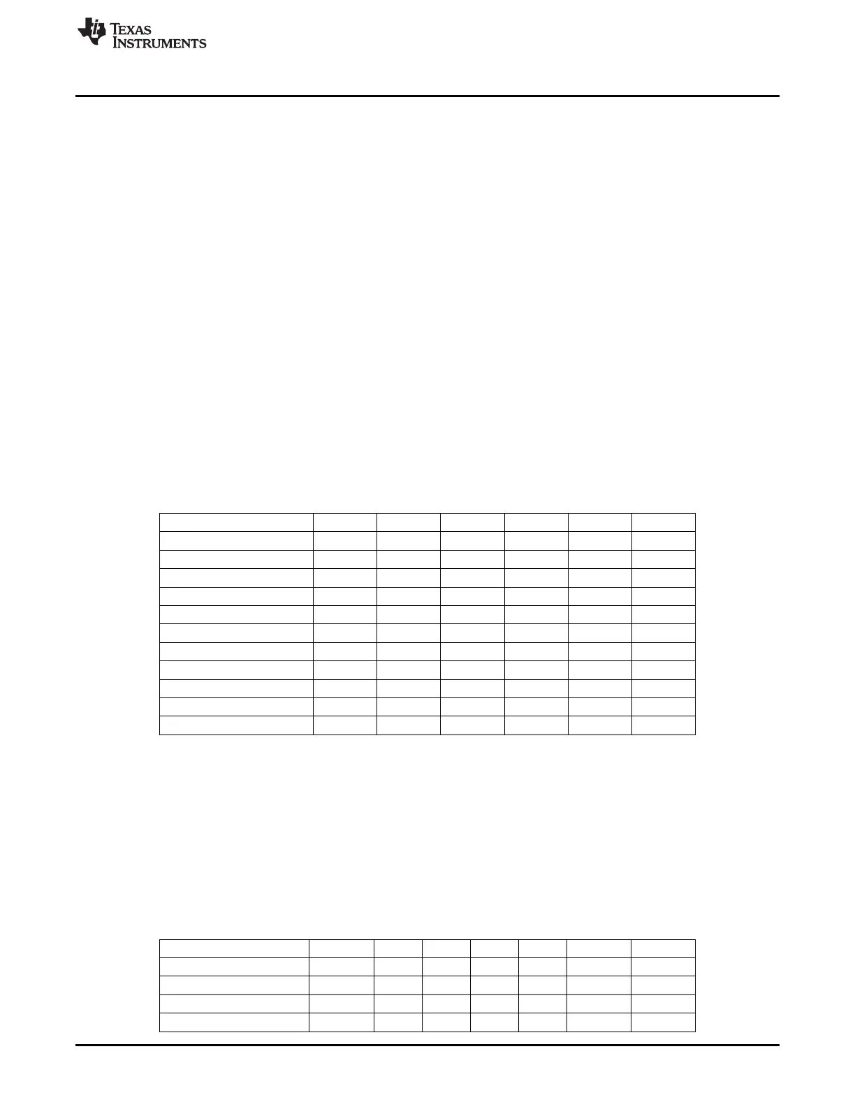
Table 7-52 summarizes the NAND interface signals level applied to external device or memories.
Table 7-52. NAND Interface Bus Operations Summary
Bus Operation CLE ALE CEn WEn REn WPn
Read (cmd input) H L L RE H x
Read (add input) L H L RE H x
Write (cmd input) H L L RE H H
Write (add input) L H L RE H H
Data input L L L RE H H
Data output L L L H FE x
Busy (during read) x x H H H x
Busy (during program) x x x x x H
Busy (during erase) x x x x x H
Write protect x x x x x L
Stand-by x x H x x H/L
7.1.4.2.3 NOR Interface Protocol
NOR flash architecture, introduced in 1988, is a flash technology. Unlike NAND, which is a sequential
access device, NOR is directly addressable; i.e., it is designed to be a random access device. NOR is
best suited to devices used to store and run code or firmware, usually in small capacities. While NOR has
fast read capabilities it has slow write and erase functions compared to NAND architecture.
Table 7-53 summarizes the NOR interface signals level applied to external device or memories.
Table 7-53. NOR Interface Bus Operations Summary
Bus Operation CLK ADVn CSn OEn WEn WAIT DQ[15:0]
Read (asynchronous) x L L L H Asserted Output
Read (synchronous) Running L L L H Driven Output
Read (burst suspend) Halted x L H H Active Output
Write x L L H L Asserted Input
363
SPRUH73H–October 2011–Revised April 2013 Memory Subsystem
Submit Documentation Feedback
Copyright © 2011–2013, Texas Instruments Incorporated

 Loading...


