Key0 = 83E7 0B13h
Key1 = 95A4 F1E0h
Locked = Write protection enabled
Unlocked = Write protection disabled
KICK1 = Any Value
or
KICK0 Key0
or
Reset
¹
KICK1 = Any Value
or
KICK0 Key0
or
Reset
¹
KICK0 = Any Value
or
KICK1 Key1¹
Reset
KICK0 = Key0
Reset
(Locked)
K0
(Locked)
K1
(Unlocked)
KICK0 = Key0 KICK1 = Key1
www.ti.com
RTC_SS
20.3.3.5 Programming/Usage Guide
20.3.3.5.1 Time/Calendar Data Format
The time and calendar data in the RTC is stored as binary-coded decimal (BCD) format. In BCD format,
the decimal numbers 0 through 9 are encoded with their binary equivalent. Although most of the
time/calendar registers have 4 bits assigned to each BCD digit, some of the register fields are shorter
since the range of valid numbers may be limited. For example, only 3 bits are required to represent the
day of the week (WEEKS_REG) since only BCD numbers 1 through 7 are required. The following time
and calendar registers are supported (BCD Format):
Note that the ALARM registers which share the names above also share the same BCD formatting.
• SECOND - Second Count (00-59)
• MINUTE - Minute Count (00-59)
• HOUR - Hour Count (12HR: 01-12; 24HR: 00-23)
• DAY - Day of the Month Count (01-31)
• WEEK - Day of the Week (0-6: SUN = 0)
• MONTH - Month Count (01-12; JAN = 1)
• YEAR - Year Count (00-99)
20.3.3.5.2 Register Access
The three register types are as follows and each has its own access constraints:
• TC and TC alarm registers
• General registers
• Compensation registers
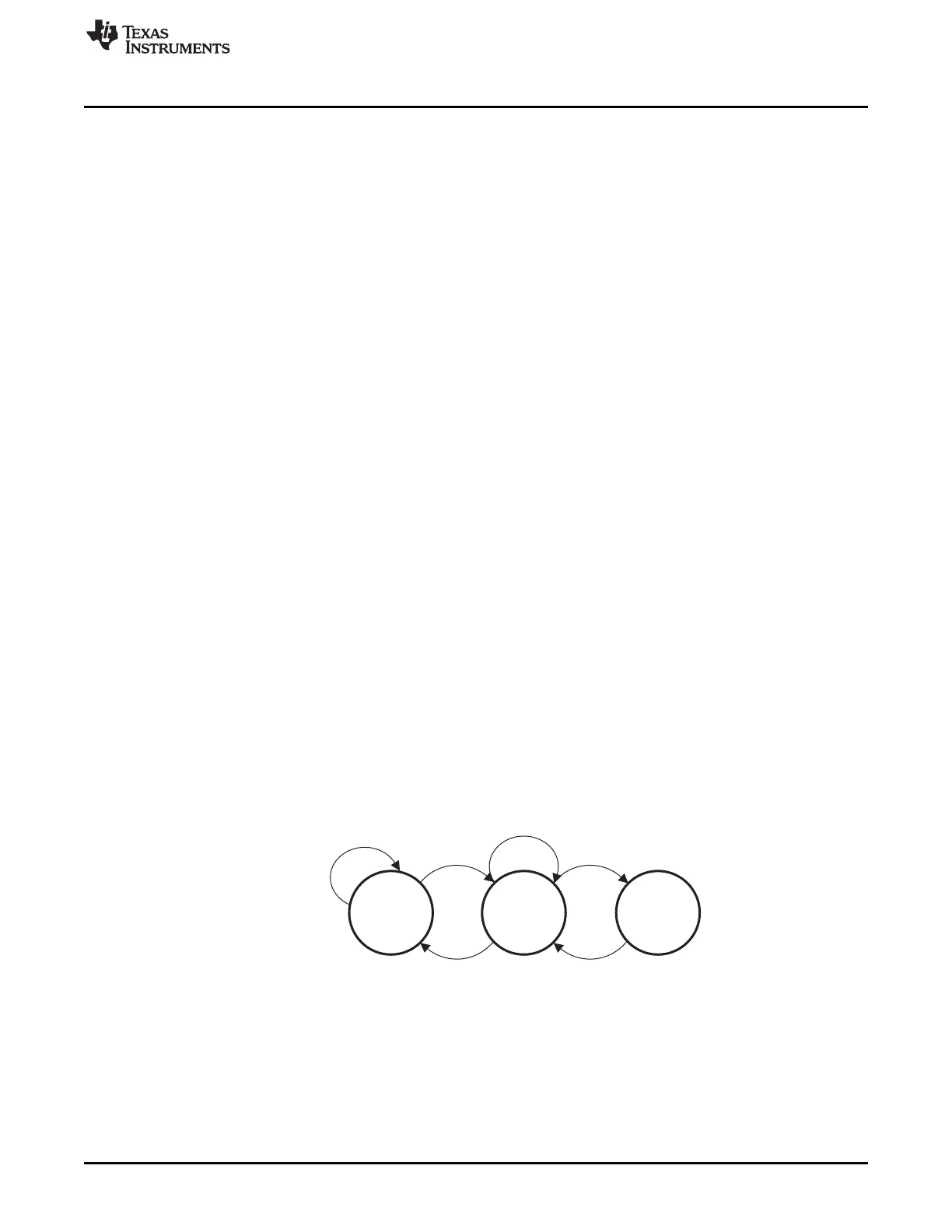
20.3.3.5.3 OCP MMR Spurious WRT Protection
The module also contains a kicker mechanism (Figure 20-58) to prevent any spurious writes from
changing the register values. This mechanism requires two MMR writes to the Kick0 and Kick1 registers
with exact data values before the kicker lock mechanism is released. Once released, the MMRs are
writeable. The Kick0 data is 83E7 0B13h; the Kick1 data is 95A4 F1E0h. Note that it remains in an
unlocked state until an OCP reset or invalid data pattern is written to one of the Kick0 or Kick1 registers.
Figure 20-58. Kick Register State Machine Diagram
3627
SPRUH73H–October 2011–Revised April 2013 Timers
Submit Documentation Feedback
Copyright © 2011–2013, Texas Instruments Incorporated

 Loading...


