Integration
www.ti.com
18.2.2 MMCHS Clock and Reset Management
The MMCHS controller has separate bus interface and functional clocks. The debounce clock is created
by dividing the 96-MHz (48 MHz @ OPP50) clock in the PRCM by two and then dividing the resulting 48-
MHz (24 MHz @ OPP50) clock by a fixed 732.4219 (366.2109 @ OPP50) in the Control Module to get a
32-kHz clock. This clock is fed back into the PRCM for clock gating. (See the CLK32KDIVRATIO_CTRL
register in Chapter 9, Control Module, for more details).
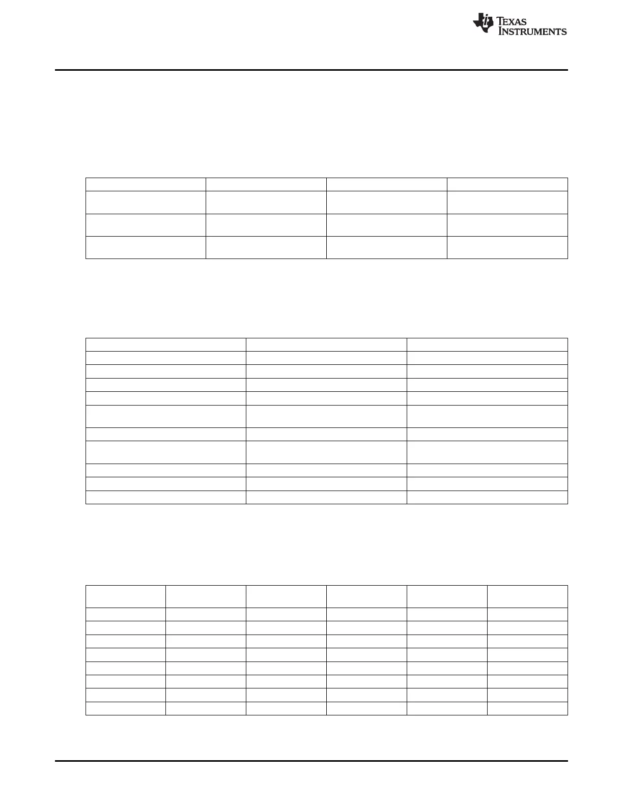
Table 18-3. MMCHS Clock Signals
Clock Signal Max Freq Reference / Source Comments
CLK 100 MHz CORE_CLKOUTM4 / 2 pd_per_l4ls_gclk
Interface clock from PRCM
CLKADPI 48 MHz PER_CLKOUTM2 / 2 pd_per_mmc_fclk
Functional clock from PRCM
CLK32 32.768 KHz CLK_24 / 732.4219 clk_32KHz
Input de-bounce clock from PRCM
18.2.3 MMCHS Pin List
The MMCHS interface pins are summarized in Table 18-4.
Table 18-4. MMCHS Pin List
Pin Type Description
MMCx_CLK I/O
(1)
MMC/SD serial clock output
MMCx_CMD I/O MMC/SD command signal
MMCx_DAT0 I/O MMC/SD data signal
MMCx_DAT1 I/O MMC/SD data signal, SDIO interrupt input
MMCx_DAT2 I/O MMC/SD data signal, SDIO read wait
output
MMCx_DAT[7:3] I/O MMC/SD data signals
MMCx_POW O MMC/SD power supply control (MMCHS 0
only)
MMCx_SDCD I SD card detect (from connector)
MMCx_SDWP I SD write protect (from connector)
MMCx_OBI I MMC out of band interrupt
(1)
This output signal is also used as a retiming input. The associated CONF_<module>_<pin>_RXACTIVE bit for the output clock
must be set to 1 to enable the clock input back to the module. It is also recommended to place a 33-ohm resistor in series (close
to the processor) to avoid signal reflections.
The direction of the data lines depends on the selected data transfer mode as summarized in Table 18-5.
Table 18-5. DAT Line Direction for Data Transfer Modes
MMC/SD MMC/SD MMC/SD SDIO SDIO
1-bit mode 4-bit mode 8-bit mode 1-bit mode 4-bit mode
DAT[0] I/O I/O I/O I/O I/O
DAT[1] I
(1)
I/O I/O I
(2)
I/O or I
(2)
DAT[2] I
(1)
I/O I/O I/O
(3)
I/O or O
(3)
DAT[3] I
(1)
I/O I/O I
(1)
I/O
DAT[4] I
(1)
I
(1)
I/O I
(1)
I
(1)
DAT[5] I
(1)
I
(1)
I/O I
(1)
I
(1)
DAT[6] I
(1)
I
(1)
I/O I
(1)
I
(1)
DAT[7] I
(1)
I
(1)
I/O I
(1)
I
(1)
(1)
Hi-Z state to avoid bus conflict.
(2)
To support incoming interrupt from the SDIO card.
(3)
To support read wait to the SDIO card. By default it is Input, Output only in read wait period.
3348
Multimedia Card (MMC) SPRUH73H–October 2011–Revised April 2013
Submit Documentation Feedback
Copyright © 2011–2013, Texas Instruments Incorporated

 Loading...


