LCD Registers
www.ti.com
13.5.9 LIDD_CS1_DATA Register (offset = 24h) [reset = 0h]
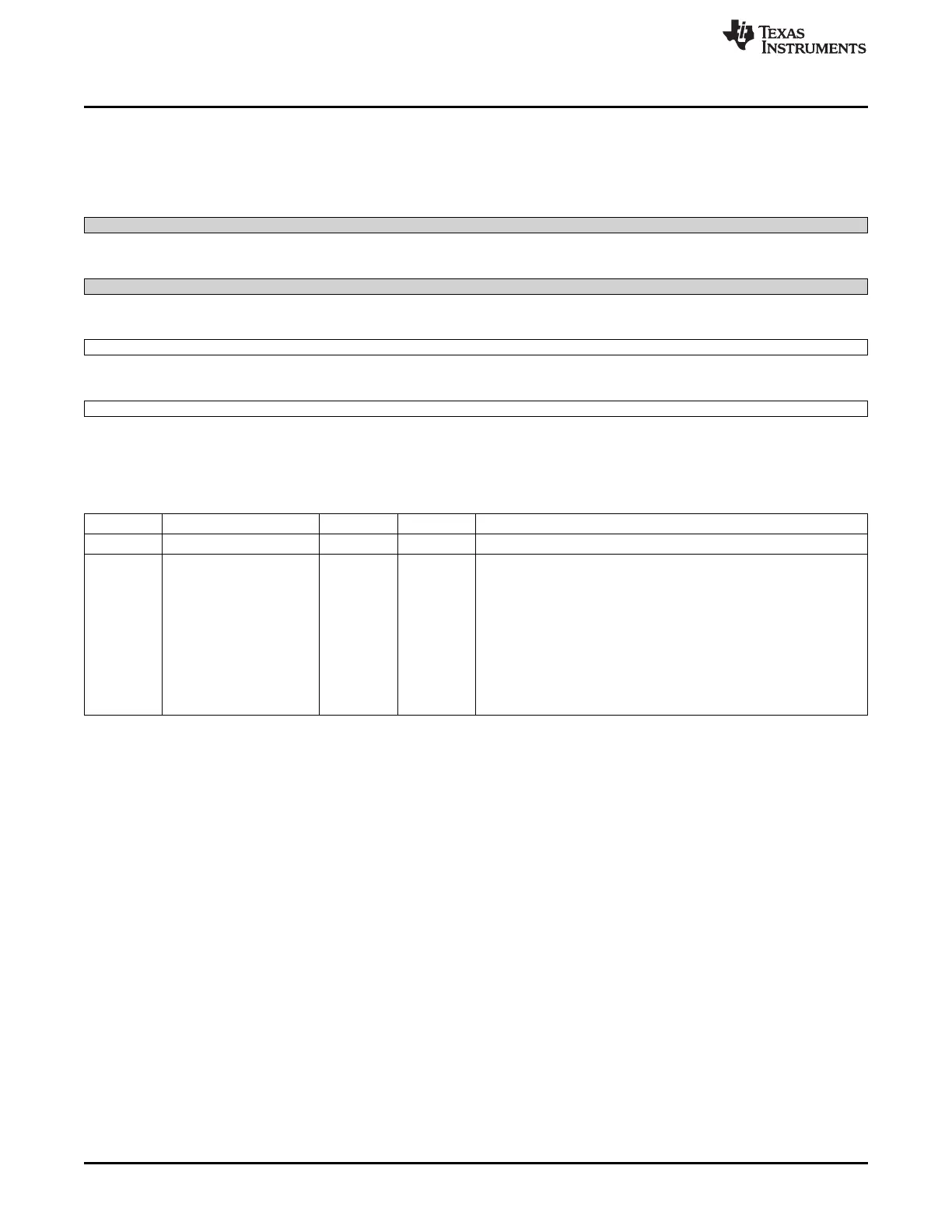
LIDD_CS1_DATA is shown in Figure 13-27 and described in Table 13-22.
Figure 13-27. LIDD_CS1_DATA Register
31 30 29 28 27 26 25 24
Reserved
R-0h
23 22 21 20 19 18 17 16
Reserved
R-0h
15 14 13 12 11 10 9 8
data
R/W-0h
7 6 5 4 3 2 1 0
data
R/W-0h
LEGEND: R/W = Read/Write; R = Read only; W1toCl = Write 1 to clear bit; -n = value after reset
Table 13-22. LIDD_CS1_DATA Register Field Descriptions
Bit Field Type Reset Description
31-16 Reserved R 0h
15-0 data R/W 0h The LCD Controller supports a shared Address/Data output bus
A write to this register would initiate a bus write transaction
A read from this register would initiate a bus read transaction
CPU reads and writes to this register are not permitted if the LIDD
module is in DMA mode (cfg_lidd_dma_en = 1)
If the LIDD is being used as a generic bus interface, writing to this
register can store adr_indx to an external transparent latch holding a
16-bit address
If the LIDD is being used to interface with a character based LCD
panel in configuration mode, reading and writing to this register can
be used to access the command instruction area of the panel
1138
LCD Controller SPRUH73H–October 2011–Revised April 2013
Submit Documentation Feedback
Copyright © 2011–2013, Texas Instruments Incorporated

 Loading...


