www.ti.com
CONTROL_MODULE Registers
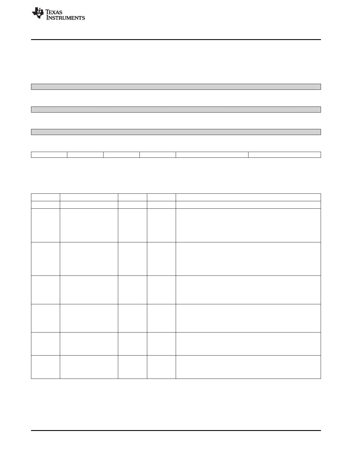
9.3.31 gmii_sel Register (offset = 650h) [reset = 0h]
gmii_sel is shown in Figure 9-34 and described in Table 9-41.
Figure 9-34. gmii_sel Register
31 30 29 28 27 26 25 24
Reserved
R-0h
23 22 21 20 19 18 17 16
Reserved
R-0h
15 14 13 12 11 10 9 8
Reserved
R-0h
7 6 5 4 3 2 1 0
rmii2_io_clk_en rmii1_io_clk_en rgmii2_idmoe rgmii1_idmode gmii2_sel gmii1_sel
R/W-0h R/W-0h R/W-0h R/W-0h R/W-0h R/W-0h
LEGEND: R/W = Read/Write; R = Read only; W1toCl = Write 1 to clear bit; -n = value after reset
Table 9-41. gmii_sel Register Field Descriptions
Bit Field Type Reset Description
31-8 Reserved R 0h
7 rmii2_io_clk_en R/W 1h 0: RMII Reference Clock Output mode. Enable RMII clock to be
sourced from PLL.
1: RMII Reference Clock Input mode. Enable RMII clock to be
sourced from chip pin.
See "Silicon Revision Functional Differences and Enhancements" for
differences in operation based on AM335x silicon revision.
6 rmii1_io_clk_en R/W 1h 0: RMII Reference Clock Output mode. Enable RMII clock to be
sourced from PLL
1: RMII Reference Clock Input mode. Enable RMII clock to be
sourced from chip pin
See "Silicon Revision Functional Differences and Enhancements" for
differences in operation based on AM335x silicon revision.
5 rgmii2_idmode R/W 1h RGMII2 Internal Delay Mode
0: Reserved
1: No Internal Delay
See "Silicon Revision Functional Differences and Enhancements" for
differences in operation based on AM335x silicon revision.
4 rgmii1_idmode R/W 1h RGMII1 Internal Delay Mode
0: Reserved
1: No Internal Delay
See "Silicon Revision Functional Differences and Enhancements" for
differences in operation based on AM335x silicon revision.
3-2 gmii2_sel R/W 0h 00: Port2 GMII/MII Mode
01: Port2 RMII Mode
10: Port2 RGMII Mode
11: Not Used
1-0 gmii1_sel R/W 0h 00: Port1 GMII/MII Mode
01: Port1 RMII Mode
10: Port1 RGMII Mode
11: Not Used
795
SPRUH73H–October 2011–Revised April 2013 Control Module
Submit Documentation Feedback
Copyright © 2011–2013, Texas Instruments Incorporated

 Loading...


