USB Registers
www.ti.com
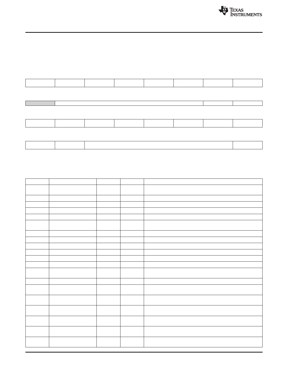
16.5.4.16 AD_INTERFACE_REG2 Register (offset = 48h) [reset = 0h]
AD_INTERFACE_REG2 is shown in Figure 16-149 and described in Table 16-160.
All bits (unless defined) are bypass bits for internal analog to digital interface pins with the same name. All
the bits of this register, except the over-ride bits return a '0' on read, if VDDLDO is off.
Figure 16-149. AD_INTERFACE_REG2 Register
31 30 29 28 27 26 25 24
USE_SUSP_DRV_RE SUS_DRV_DP_DATA SUS_DRV_DP_EN SUS_DRV_DM_DATA SUS_DRV_DM_EN USE_DISCON_REG DISCON_EN DISCON_PRE_EN
G
R/W-0h R/W-0h R/W-0h R/W-0h R/W-0h R/W-0h R/W-0h R/W-0h
23 22 21 20 19 18 17 16
Reserved SPARE_OUT_CORE SERX_DP_CORE SERX_DM_CORE
R/W-0h R-0h R-0h R-0h
15 14 13 12 11 10 9 8
USE_HSRX_CAL_EN HSRX_CAL_EN USE_RPU_RPD_RE RPU_DP_SW1_EN_C RPU_DP_SW2_EN_C RPU_DM_SW1_EN_ RPU_DM_SW2_EN_ DP_PULLDOWN_EN
_REG G ORE ORE CORE CORE _CORE
R/W-0h R/W-0h R/W-0h R/W-0h R/W-0h R/W-0h R/W-0h R/W-0h
7 6 5 4 3 2 1 0
DM_PULLDOWN_EN DP_DM_5V_SHORT SPARE_IN_CORE PORZ
_CORE
R/W-0h R-0h R/W-0h R-0h
LEGEND: R/W = Read/Write; R = Read only; W1toCl = Write 1 to clear bit; -n = value after reset
Table 16-160. AD_INTERFACE_REG2 Register Field Descriptions
Bit Field Type Reset Description
31 USE_SUSP_DRV_REG R/W 0h Use bits
27-30 from this register as overrides
30 SUS_DRV_DP_DATA R/W 0h
29 SUS_DRV_DP_EN R/W 0h
28 SUS_DRV_DM_DATA R/W 0h
27 SUS_DRV_DM_EN R/W 0h
26 USE_DISCON_REG R/W 0h Use bits
24-25 from this register as override
25 DISCON_EN R/W 0h
24 DISCON_PRE_EN R/W 0h
23 Reserved R/W 0h
22-18 SPARE_OUT_CORE R 0h
17 SERX_DP_CORE R 0h
16 SERX_DM_CORE R 0h
15 USE_HSRX_CAL_EN_RE R/W 0h
Use bit 14 from this register as override
G
14 HSRX_CAL_EN R/W 0h
13 USE_RPU_RPD_REG R/W 0h Use override from bits
7-12
12 RPU_DP_SW1_EN_COR R/W 0h
E
11 RPU_DP_SW2_EN_COR R/W 0h
E
10 RPU_DM_SW1_EN_COR R/W 0h
E
9 RPU_DM_SW2_EN_COR R/W 0h
E
8 DP_PULLDOWN_EN_CO R/W 0h
RE
1922
Universal Serial Bus (USB) SPRUH73H–October 2011–Revised April 2013
Submit Documentation Feedback
Copyright © 2011–2013, Texas Instruments Incorporated

 Loading...


