EMIF
www.ti.com
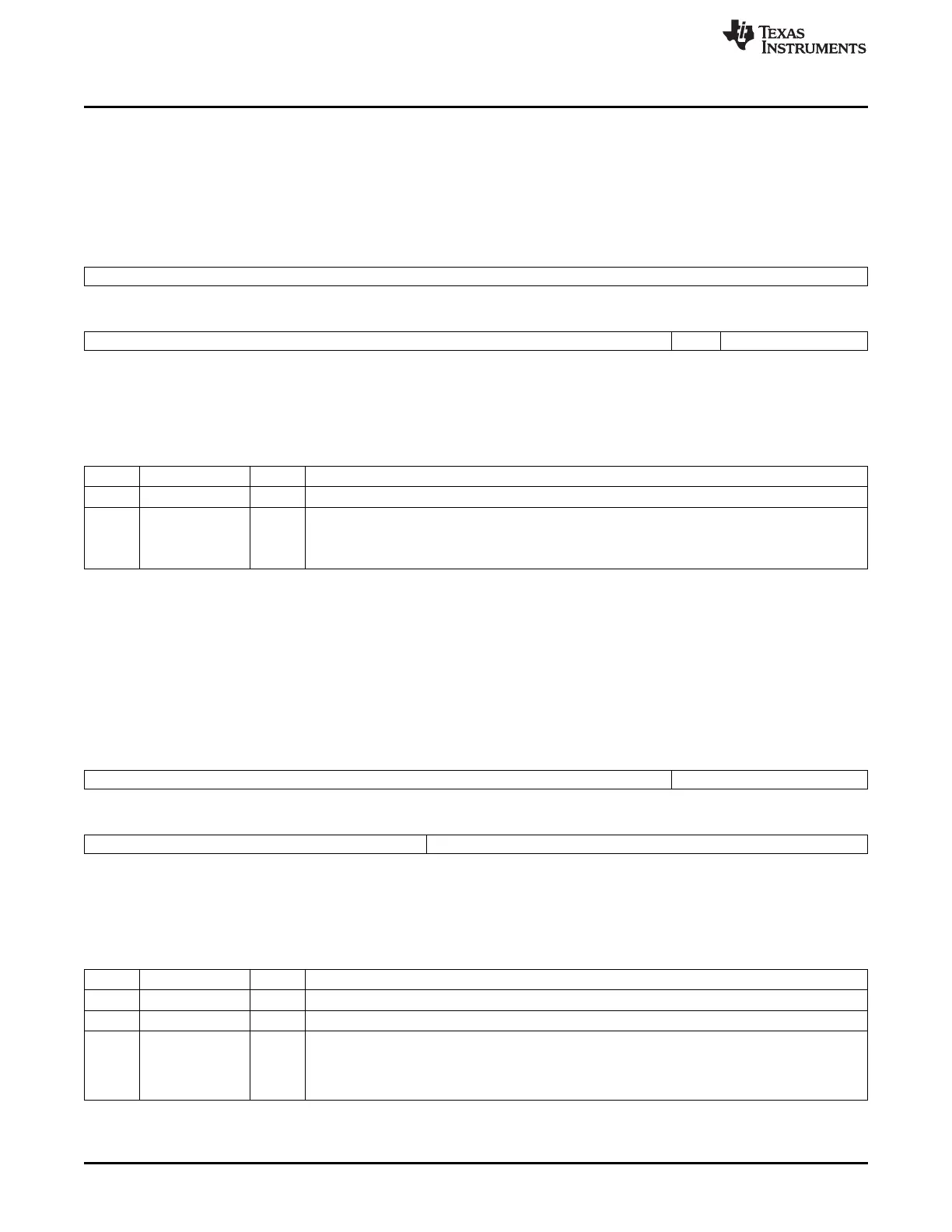
7.3.6.3 DDR PHY Command 0/1/2 Invert Clockout Selection Register(
CMD0/1/2_REG_PHY_INVERT_CLKOUT_0)
The CDDR PHY Command 0/1/2 Invert Clockout Selection Register(
CMD0/1/2_REG_PHY_INVERT_CLKOUT_0) is shown in the figure and table below.
Figure 7-131. DDR PHY Command 0/1/2 Invert Clockout Selection Register(
CMD0/1/2_REG_PHY_INVERT_CLKOUT_0)
31 16
Reserved
R-0
15 1 0
Reserved INVERT_CLK_SEL
R-0 W-0
LEGEND: R/W = Read/Write; R = Read only; -n = value after reset
Table 7-152. DDR PHY Command 0/1/2 Invert Clockout Selection Register(
CMD0/1/2_REG_PHY_INVERT_CLKOUT_0) Field Descriptions
Bit Field Value Description
31-1 Reserved 0 Reserved
0 INVERT_CLK_SE Inverts the polarity of DRAM clock.
L
0 Core clock is passed on to DRAM
1 inverted core clock is passed on to DRAM
7.3.6.4 DDR PHY Data Macro 0/1 Read DQS Slave Ratio Register
(DATA0/1_REG_PHY_RD_DQS_SLAVE_RATIO_0)
The DDR PHY Data Macro 0/1 Read DQS Slave Ratio
Register(DATA0/1_REG_PHY_RD_DQS_SLAVE_RATIO_0) is shown in the figure and table below.
Figure 7-132. DDR PHY Data Macro 0/1 Read DQS Slave Ratio Register
(DATA0/1_REG_PHY_RD_DQS_SLAVE_RATIO_0))
31 i 19 16
Reserved Reserved
R-0h R-0h
15 10 9 0
Reserved RD_DQS_SLAVE_RATIO_CS0
R-0h W-40h
LEGEND: R/W = Read/Write; R = Read only; -n = value after reset
Table 7-153. DDR PHY Data Macro 0/1 Read DQS Slave Ratio Register
(DATA0/1_REG_PHY_RD_DQS_SLAVE_RATIO_0) Field Descriptions
Bit Field Value Description
31-20 Reserved Reserved
19-10 Reserved 0h Reserved
9-0 RD_DQS_SLAVE Ratio value for Read DQS slave DLL for CS0.
_RATIO_CS0
40h This is the fraction of a clock cycle represented by the shift to be applied to the read DQS in units of
256ths. In other words, the full-cycle tap value from the master DLL will be scaled by this number
over 256 to get the delay value for the slave delay line.
470
Memory Subsystem SPRUH73H–October 2011–Revised April 2013
Submit Documentation Feedback
Copyright © 2011–2013, Texas Instruments Incorporated

 Loading...


