www.ti.com
EMIF
7.3.5.9 SDRAM_TIM_2 Register (offset = 20h) [reset = 0h]
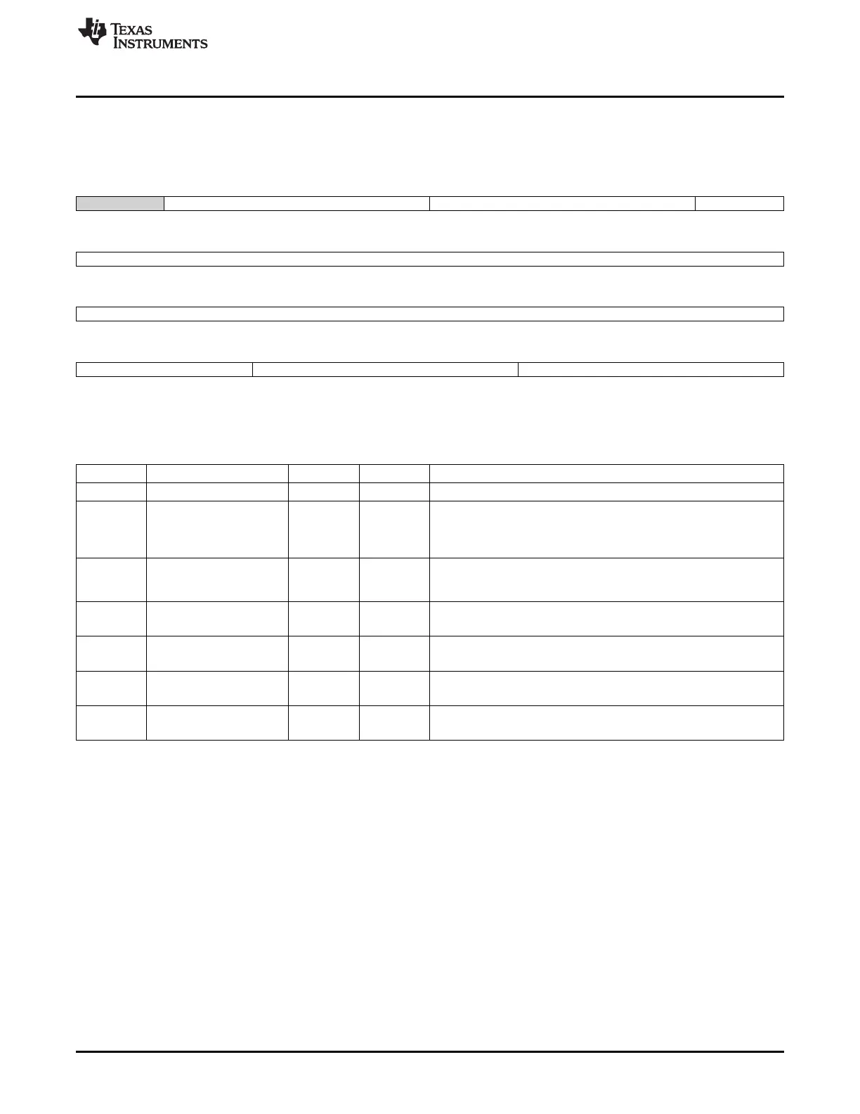
SDRAM_TIM_2 is shown in Figure 7-99 and described in Table 7-119.
Figure 7-99. SDRAM_TIM_2 Register
31 30 29 28 27 26 25 24
Reserved reg_t_xp reg_t_odt reg_t_xsnr
R-0h R/W-0h R/W-0h R/W-0h
23 22 21 20 19 18 17 16
reg_t_xsnr
R/W-0h
15 14 13 12 11 10 9 8
reg_t_xsrd
R/W-0h
7 6 5 4 3 2 1 0
reg_t_xsrd reg_t_rtp reg_t_cke
R/W-0h R/W-0h R/W-0h
LEGEND: R/W = Read/Write; R = Read only; W1toCl = Write 1 to clear bit; -n = value after reset
Table 7-119. SDRAM_TIM_2 Register Field Descriptions
Bit Field Type Reset Description
31 Reserved R 0h
30-28 reg_t_xp R/W 0h Minimum number of DDR clock cycles from Powerdown exit to any
command other than a Read command, minus one.
For DDR2 and LPDDR1, this field must satisfy greater of tXP or
tCKE.
27-25 reg_t_odt R/W 0h Minimum number of DDR clock cycles from ODT enable to write
data driven for DDR2 and DDR3.
reg_t_odt must be equal to tAOND.
24-16 reg_t_xsnr R/W 0h
Minimum number of DDR clock cycles from Self-Refresh exit to any
command other than a Read command, minus one.
15-6 reg_t_xsrd R/W 0h
Minimum number of DDR clock cycles from Self-Refresh exit to a
Read command, minus one.
5-3 reg_t_rtp R/W 0h
Minimum number of DDR clock cycles from the last Read command
to a Pre-charge command for DDR2 and DDR3, minus one.
2-0 reg_t_cke R/W 0h
Minimum number of DDR clock cycles between pad_cke_o changes,
minus one.
433
SPRUH73H–October 2011–Revised April 2013 Memory Subsystem
Submit Documentation Feedback
Copyright © 2011–2013, Texas Instruments Incorporated

 Loading...


