www.ti.com
EMIF
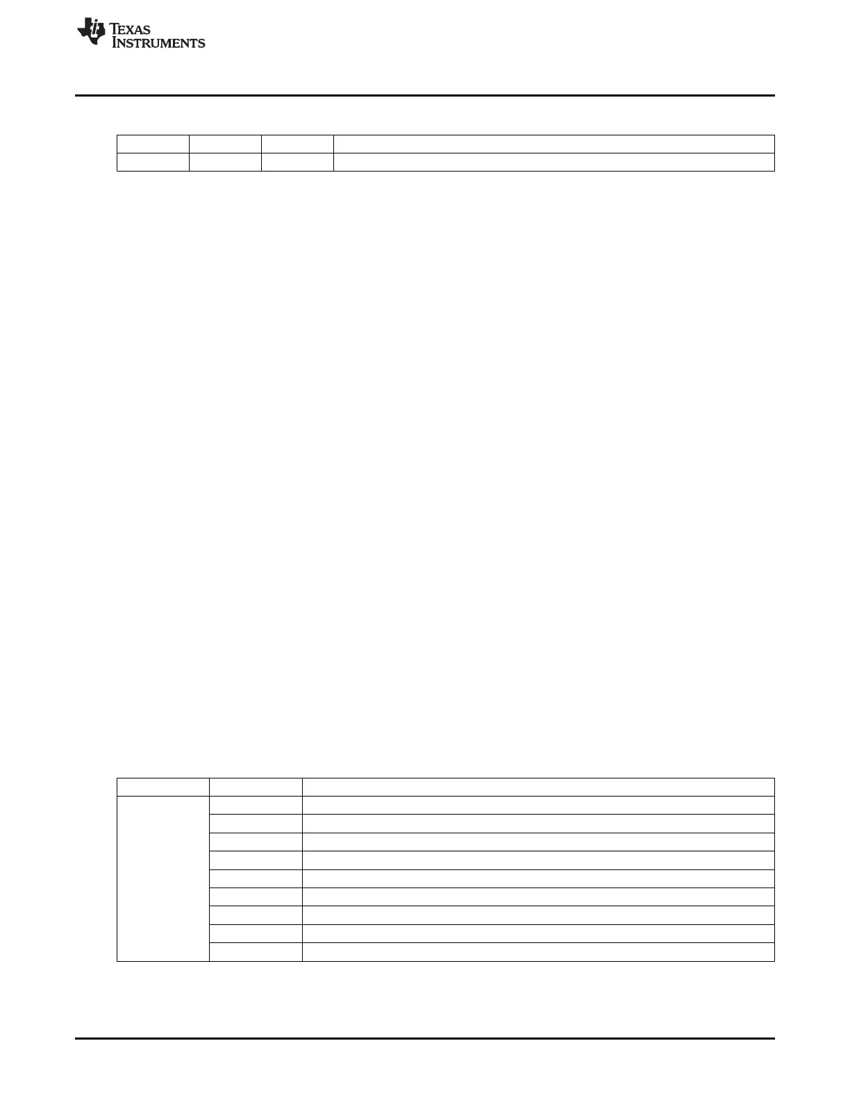
Table 7-98. Digital Filter Configuration (continued)
F2 F1 F0 Description
1 1 1 Update on 8 consecutive update requests
7.3.3.3.5 DQS-Gate IOs
To effectively model the I/O delay on the DQS gating signal during a read request (the DQS receiver and
the CLK driver I/Os), the signal is expected to be looped on a single I/O connecting fifo_we_in to
fifo_we_out. The board and memory delay, being fairly constant across PTV variations, are calibrated
within the IDID using a compensated delay line. The loop-back is done at the die level without bringing the
signals out to the package level. Each Data Macro supports delay compensation independent of each
other.
The data and command macros are responsible for System level flight time compensation. The following
controls are supported by the DDR2/3/mDDR controller Sub System.
• Aligning DDR_DQS w.r.t DDR_CLK during Write Cycle: For DDR3 operation, initiate the write leveling
state machine on each rank in turn to capture the proper delay settings to align DDR_DQS with
DDR_CLK clock for each memory chip. If one wants to do this in a manual way one can write to the
control register that controls the delay of DDR_DQS vs DDR_CLK Clock position. To produce a given
amount of skew to center the DDR_DQS vs. Clock at the SDRAM the following register can be
programmed.
Data Macro 0/1 Write DQS Slave Ratio Register=256 x ([command delay] – [DDR_DQS delay]) /
DDR_CLK Clock period.
• Aligning ADDR/CMD w.r.t DDR_CLK
• Aligning DDR_DQ[15:0] w.r.t DDR_DQS during Write Operation
• Offset DDR_D[15:0] w.r.t DDR_DQS during Read Operation
• Align FIFO WE Window
7.3.3.4 Address Mapping
The DDR2/3/mDDR memory controller views external DDR2/3/mDDR SDRAM as one continuous block of
memory. This statement is true regardless of the number of memory devices located on the chip select
space. The DDR2/3/mDDR memory controller receives DDR2/3/mDDR memory access requests along
with a 32-bit logical address from the rest of the system. In turn, DDR2/3/mDDR memory controller uses
the logical address to generate a row/page, column, and bank address for the DDR2/3/mDDR SDRAM.
The number of column, row and bank address bits used is determined by the IBANK, RSIZE and
PAGESIZE fields (see Table 7-99). The DDR2/3/mDDR memory controller uses up to 16 bits for the
row/page address.
Table 7-99. IBANK, RSIZE and PAGESIZE Fields Information
Bit Field Bit Value Bit Description
Defines the number of address lines to be connected to DDR2/3/mDDR memory device
0 9 row bits
1h 10 row bits
2h 11 row bits
RSIZE 3h 12 row bits
4h 13 row bits
5h 14 row bits
6h 15 row bits
7h 16 row bits
409
SPRUH73H–October 2011–Revised April 2013 Memory Subsystem
Submit Documentation Feedback
Copyright © 2011–2013, Texas Instruments Incorporated

 Loading...


