www.ti.com
Power, Reset, and Clock Management
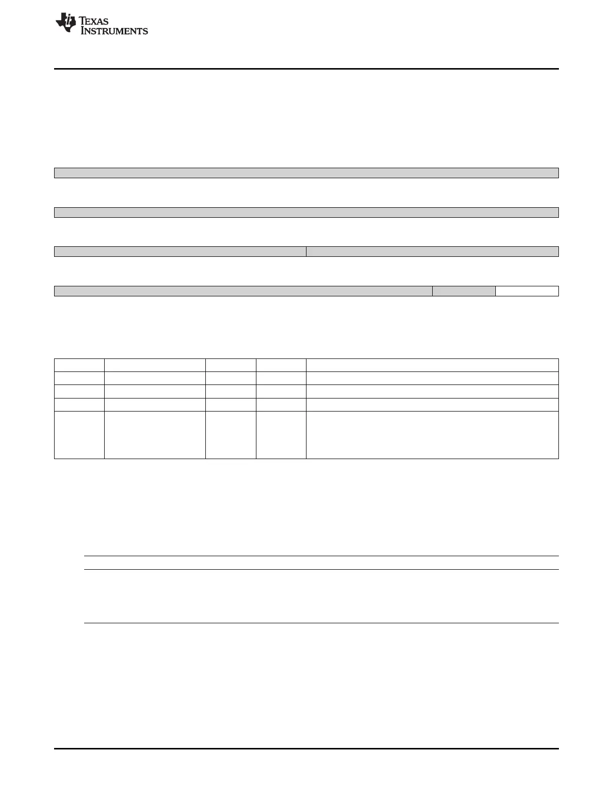
8.1.13.7.4 RM_GFX_RSTST Register (offset = 14h) [reset = 0h]
RM_GFX_RSTST is shown in Figure 8-192 and described in Table 8-213.
This register logs the different reset sources of the GFX domain. Each bit is set upon release of the
domain reset signal. Must be cleared by software. [warm reset insensitive]
Figure 8-192. RM_GFX_RSTST Register
31 30 29 28 27 26 25 24
Reserved
R-0h
23 22 21 20 19 18 17 16
Reserved
R-0h
15 14 13 12 11 10 9 8
Reserved Reserved
R-0h R-0h
7 6 5 4 3 2 1 0
Reserved Reserved GFX_RST
R-0h R-0h R/W-0h
LEGEND: R/W = Read/Write; R = Read only; W1toCl = Write 1 to clear bit; -n = value after reset
Table 8-213. RM_GFX_RSTST Register Field Descriptions
Bit Field Type Reset Description
31-12 Reserved R 0h
11-2 Reserved R 0h
1 Reserved R 0h
0 GFX_RST R/W 0h
GFX Domain Logic Reset
0x0 = RESET_NO : No SW reset occured
0x1 = RESET_YES : GFX Domain Logic has been reset upon SW
reset
8.1.13.8 PRM_CEFUSE Registers
Table 8-214 lists the memory-mapped registers for the PRM_CEFUSE. All register offset addresses not
listed in Table 8-214 should be considered as reserved locations and the register contents should not be
modified.
Table 8-214. PRM_CEFUSE REGISTERS
Offset Acronym Register Name Section
0h PM_CEFUSE_PWRSTCTRL This register controls the CEFUSE power state to reach Section 8.1.13.8.1
upon a domain sleep transition
4h PM_CEFUSE_PWRSTST This register provides a status on the current CEFUSE Section 8.1.13.8.2
power domain state.
[warm reset insensitive]
743
SPRUH73H–October 2011–Revised April 2013 Power, Reset, and Clock Management (PRCM)
Submit Documentation Feedback
Copyright © 2011–2013, Texas Instruments Incorporated

 Loading...


