EDMA3 Registers
www.ti.com
11.4.2.7.10 Destination FIFO Options Register (DFOPTn)
The destination FIFO options register (DFOPTn) is shown in Figure 11-124 and described in Table 11-
109.
NOTE: The value for n varies from 0 to DSTREGDEPTH for the given EDMA3TC.
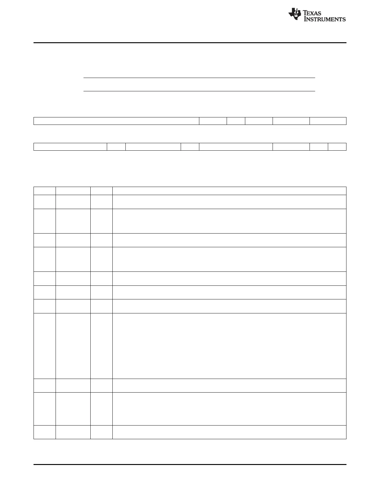
Figure 11-124. Destination FIFO Options Register (DFOPTn)
31 23 22 21 20 19 18 17 16
Reserved TCCHEN Rsvd TCINTEN Reserved TCC
R-0 R/W-0 R-0 R/W-0 R-0 R/W-0
15 12 11 10 8 7 6 4 3 2 1 0
TCC Rsvd FWID Rsvd PRI Reserved DAM SAM
R/W-0 R-0 R/W-0 R-0 R/W-0 R-0 R/W-0 R/W-0
LEGEND: R/W = Read/Write; R = Read only; -n = value after reset
Table 11-109. Destination FIFO Options Register (DFOPTn) Field Descriptions
Bit Field Value Description
31-23 Reserved 0 Reserved. Always write 0 to this bit; writes of 1 to this bit are not supported and attempts to do so may
result in undefined behavior.
22 TCCHEN Transfer complete chaining enable
0 Transfer complete chaining is disabled
1 Transfer complete chaining is enabled
21 Reserved 0 Reserved. Always write 0 to this bit; writes of 1 to this bit are not supported and attempts to do so may
result in undefined behavior.
20 TCINTEN Transfer complete interrupt enable.
0 Transfer complete interrupt is disabled.
1 Transfer complete interrupt is enabled.
19-18 Reserved 0 Reserved. Always write 0 to this bit; writes of 1 to this bit are not supported and attempts to do so may
result in undefined behavior.
17-12 TCC 0-3Fh Transfer complete code. This 6-bit code is used to set the relevant bit in CER or IPR of the EDMA3PCC
module.
11 Reserved 0 Reserved. Always write 0 to this bit; writes of 1 to this bit are not supported and attempts to do so may
result in undefined behavior.
10-8 FWID 0-7h FIFO width. Applies if either SAM or DAM is set to constant addressing mode.
0 FIFO width is 8-bit.
1h FIFO width is 16-bit.
2h FIFO width is 32-bit.
3h FIFO width is 64-bit.
4h FIFO width is 128-bit.
5h FIFO width is 256-bit.
6h-7h Reserved.
7 Reserved 0 Reserved. Always write 0 to this bit; writes of 1 to this bit are not supported and attempts to do so may
result in undefined behavior.
6-4 PRI 0-7h Transfer priority
0 Priority 0 - Highest priority
1h-6h Priority 1 to priority 6
7h Priority 7 - Lowest priority
3-2 Reserved 0 Reserved. Always write 0 to this bit; writes of 1 to this bit are not supported and attempts to do so may
result in undefined behavior.
1012
Enhanced Direct Memory Access (EDMA) SPRUH73H–October 2011–Revised April 2013
Submit Documentation Feedback
Copyright © 2011–2013, Texas Instruments Incorporated

 Loading...


