www.ti.com
GPMC
7.1.4.1.3 GPMC Configuration for Synchronous Burst Read Access
The clock runs at 104 MHz ( f = 104 MHz; T = 9, 615 ns).
Table 7-46 shows the timing parameters (on the memory side) that determine the parameters on the
GPMC side.
Table 7-47 shows how to calculate timings for the GPMC using the memory parameters.
Figure 7-48 shows the synchronous burst read access.
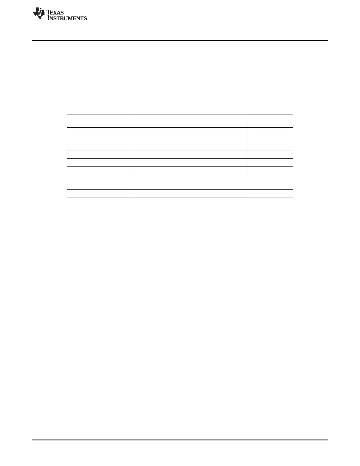
Table 7-46. Useful Timing Parameters on the Memory Side
AC Read Characteristics
Description Duration (ns)
on the Memory Side
tCES CSn setup time to clock 0
tACS Address setup time to clock 3
tIACC Synchronous access time 80
tBACC Burst access time valid clock to output delay 5,2
tCEZ Chip-select to High-Impedance 7
tOEZ Output enable to High-Impedance 7
tAVC ADVn setup time 6
tAVD AVDn pulse 6
tACH Address hold time from clock 3
The following terms, which describe the timing interface between the controller and its attached device,
are used to calculate the timing parameters on the GPMC side:
• Read Access time (GPMC side): Time required to activate the clock + read access time requested on
the memory side + data setup time required for optimal capture of a burst of data
• Data setup time (GPMC side): Ensures a good capture of a burst of data (as opposed to taking a burst
of data out). One word of data is processed in one clock cycle (T = 9,615 ns). The read access time
between 2 bursts of data is tBACC = 5,2 ns. Therefore, data setup time is a clock period - tBACC =
4,415 ns of data setup.
• Access completion (GPMC side): (Different from page burst access time) Time required between the
last burst access and access completion: CSn/OEn hold time (CSn and OEn must be released at the
end of an access. These signals are held to allow the access to complete).
• Read cycle time (GPMC side): Read Access time + access completion
• Write cycle time for burst access: Not supported for NOR flash memory
357
SPRUH73H–October 2011–Revised April 2013 Memory Subsystem
Submit Documentation Feedback
Copyright © 2011–2013, Texas Instruments Incorporated

 Loading...


