SPI Shift Clock
(Module Generated
Internal Clock)
SPICLKO
(POL=1)
SPIENO
SPICLKO
(POL=0)
TCS = 0.5
TCS = 1.5
TCS = 2.5
TCS = 3.5
TCS = 0.5
TCS = 1.5
TCS = 2.5
TCS = 3.5
www.ti.com
Functional Description
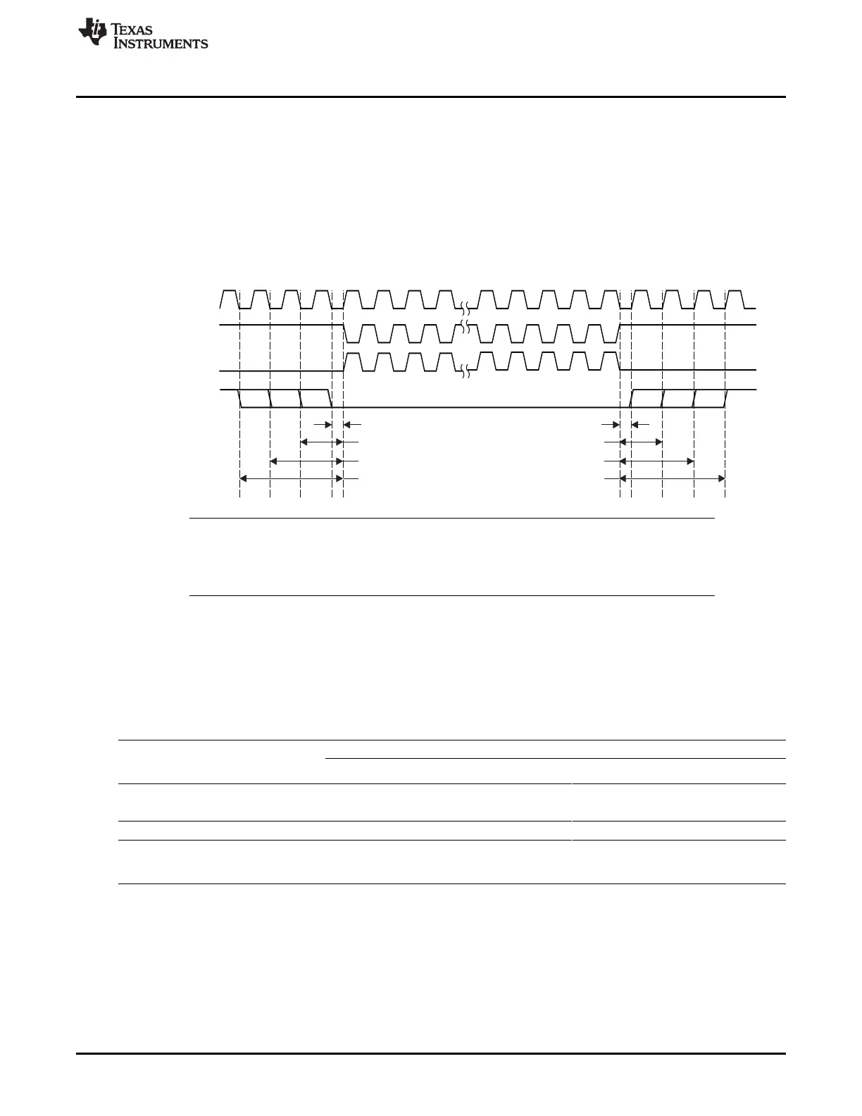
24.3.2.8 Chip-Select Timing Control
The chip select timing control is only available in master mode with automatic chip select generation
(FORCE bit field is cleared to 0), to add a programmable delay between chip select assertion and first
clock edge or chip select removal and last clock edge. The option is available only in 4 pin mode
MCSPI_MODULCTRL[1] PIN34 is cleared to 0.
This mode is programmable per channel (bit TCS of the register MCSPI_CH(I)CONF). Figure 24-12
shows the chip-select SPIEN timing control.
Figure 24-12. Chip-Select SPIEN Timing Controls
NOTE: Because of the design implementation for transfers using a clock divider ratio set to 1 (clock
bypassed), a half cycle must be added to the value between chip-select assertion and the
first clock edge with PHA = 1 or between chip-select removal and the last clock edge with
PHA = 0.
With an odd clock divider ratio which occurs when granularity is one clock cycle, that means that
MCSPI_CH(I)CONF[CLKG] is set to 1 and MCSPI_CH(I)CONF[CLKD] has an even value, the clock duty
cycle is not 50%, then one of the high level or low level duration is selected to be added to TCS delay.
Table 24-6 summarizes all delays between chip select and first (setup) or last (hold) clock edge.
In 3-pin mode this option is useless, the chip select SPIEN is forced to low state.
Table 24-6. Chip Select ↔ Clock Edge Delay Depending on Configuration
Clock Ratio F
ratio
Clock Chip Select ↔ Clock Edge Delay
Phase
Setup Hold
PHA
1 0 T_ref × (TCS + ½) T_ref × (TCS + 1)
1 T_ref × (TCS + 1) T_ref × (TCS + ½)
Even ≥ 2 x T_ref × F
ratio
× (TCS + ½) T_ref × F
ratio
× (TCS + ½)
Odd ≥ 3 (only with 0 T_ref × [{F
ratio
× TCS) + (F
ratio
+ ½)] T_ref × [{F
ratio
× TCS) + (F
ratio
+ ½)]
MCSPI_CH(I)CONF[CLK
1 T_ref × [{F
ratio
× TCS) + (F
ratio
- ½)] T_ref × [{F
ratio
× TCS) + (F
ratio
- ½)]
G] set to 1
T_ref = CLKSPIREF period in ns. F
ratio
= SPI clock division ratio
The clock divider ratio depends on divider granularity MCSPI_CH(I)CONF[CLKG]:
• MCSPI_CH(I)CONF[CLKG] = 0 : granularity is power of two.
F
ratio
= 2
MCSPI_CH(I)CONF[CLKD]
• MCSPI_CH(I)CONF[CLKG] = 0 : granularity is power of two.
4011
SPRUH73H–October 2011–Revised April 2013 Multichannel Serial Port Interface (McSPI)
Submit Documentation Feedback
Copyright © 2011–2013, Texas Instruments Incorporated

 Loading...


