Power, Reset, and Clock Management
www.ti.com
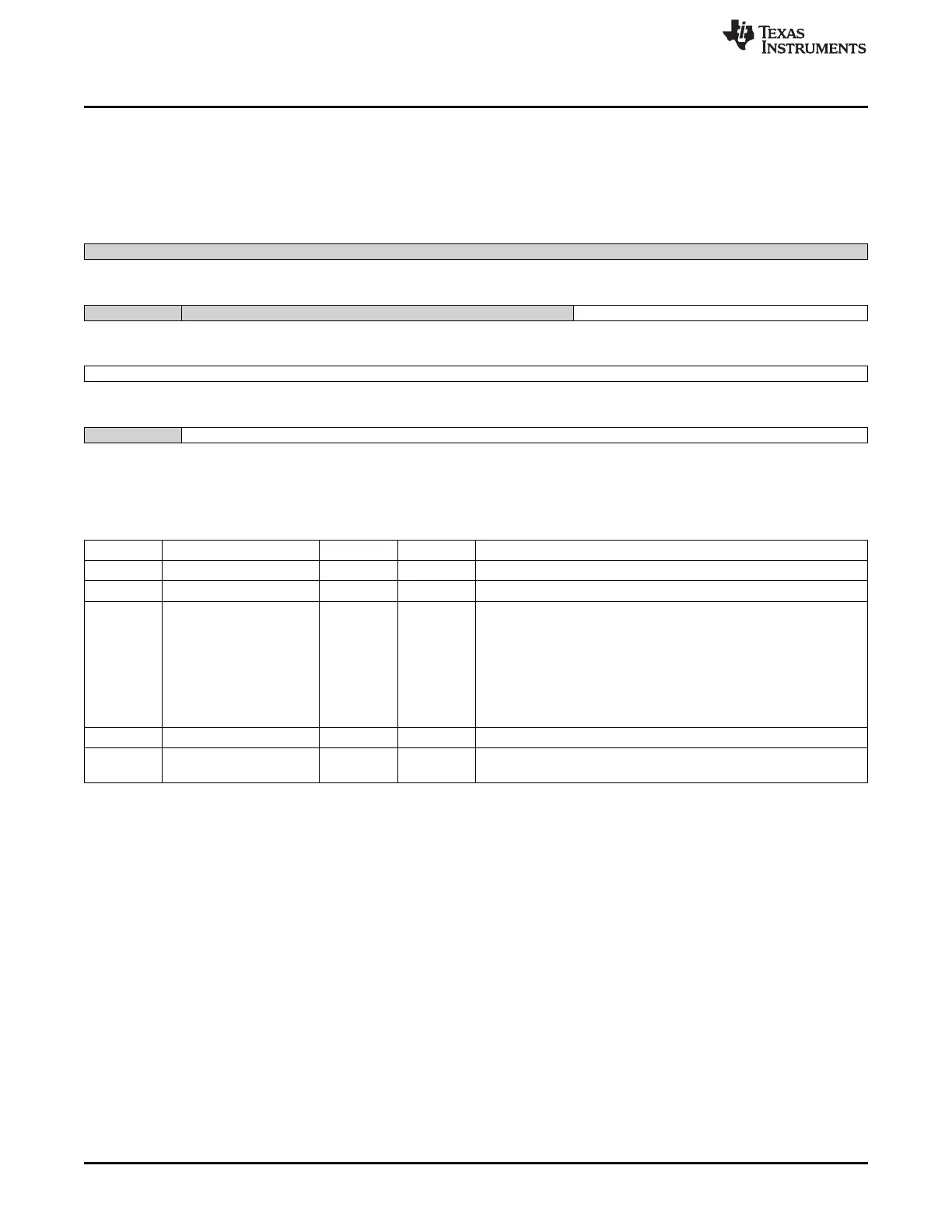
8.1.12.2.27 CM_CLKSEL_DPLL_CORE Register (offset = 68h) [reset = 0h]
CM_CLKSEL_DPLL_CORE is shown in Figure 8-110 and described in Table 8-118.
This register provides controls over the DPLL.
Figure 8-110. CM_CLKSEL_DPLL_CORE Register
31 30 29 28 27 26 25 24
Reserved
R-0h
23 22 21 20 19 18 17 16
Reserved Reserved DPLL_MULT
R-0h R-0h R/W-0h
15 14 13 12 11 10 9 8
DPLL_MULT
R/W-0h
7 6 5 4 3 2 1 0
Reserved DPLL_DIV
R-0h R/W-0h
LEGEND: R/W = Read/Write; R = Read only; W1toCl = Write 1 to clear bit; -n = value after reset
Table 8-118. CM_CLKSEL_DPLL_CORE Register Field Descriptions
Bit Field Type Reset Description
31-23 Reserved R 0h
22-19 Reserved R 0h
18-8 DPLL_MULT R/W 0h DPLL multiplier factor (2 to 2047).
This register is automatically cleared to 0 when the DPLL_EN field in
the *CLKMODE_DPLL* register is set to select MN Bypass mode.
(equal to input M of DPLL
M=2 to
2047 => DPLL multiplies by M)
0x0 = Reserved_0 : Reserved
0x1 = Reserved_1 : Reserved
7 Reserved R 0h
6-0 DPLL_DIV R/W 0h DPLL divider factor (0 to 127) (equal to input N of DPLL
actual division factor is N+1).
642
Power, Reset, and Clock Management (PRCM) SPRUH73H–October 2011–Revised April 2013
Submit Documentation Feedback
Copyright © 2011–2013, Texas Instruments Incorporated

 Loading...


