www.ti.com
Power, Reset, and Clock Management
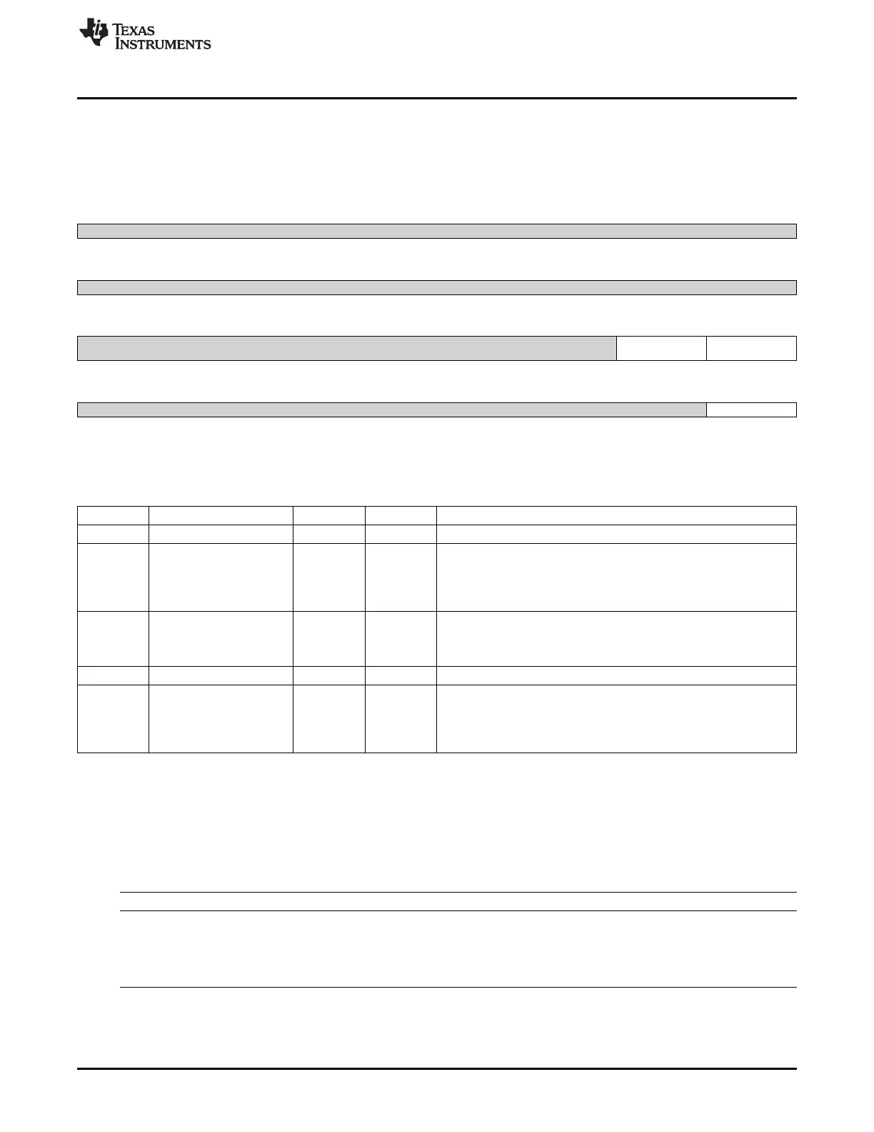
8.1.13.5.8 PRM_LDO_SRAM_MPU_CTRL Register (offset = 1Ch) [reset = 0h]
PRM_LDO_SRAM_MPU_CTRL is shown in Figure 8-186 and described in Table 8-205.
Control and status of the SRAM LDO for MPU voltage domain. [warm reset insensitive]
Figure 8-186. PRM_LDO_SRAM_MPU_CTRL Register
31 30 29 28 27 26 25 24
Reserved
R-0h
23 22 21 20 19 18 17 16
Reserved
R-0h
15 14 13 12 11 10 9 8
Reserved SRAM_IN_TRANSITI SRAMLDO_STATUS
ON
R-0h R-0h R-0h
7 6 5 4 3 2 1 0
Reserved RETMODE_ENABLE
R-0h R/W-0h
LEGEND: R/W = Read/Write; R = Read only; W1toCl = Write 1 to clear bit; -n = value after reset
Table 8-205. PRM_LDO_SRAM_MPU_CTRL Register Field Descriptions
Bit Field Type Reset Description
31-10 Reserved R 0h
9 SRAM_IN_TRANSITION R 0h
Status indicating SRAM LDO state machine state.
0x0 = IDLE : SRAM LDO state machine is stable
0x1 = IN_TRANSITION : SRAM LDO state machine is in transition
state
8 SRAMLDO_STATUS R 0h
SRAMLDO status
0x0 = ACTIVE : SRAMLDO is in ACTIVE mode.
0x1 = RETENTION : SRAMLDO is on RETENTION mode.
7-1 Reserved R 0h
0 RETMODE_ENABLE R/W 0h
Control if the SRAM LDO retention mode is used or not.
0x0 = Disabled : SRAM LDO is not allowed to go to RET mode
0x1 = Enabled : SRAM LDO go to RET mode when all memory of
voltage domain are OFF or RET
8.1.13.6 PRM_RTC Registers
Table 8-206 lists the memory-mapped registers for the PRM_RTC. All register offset addresses not listed
in Table 8-206 should be considered as reserved locations and the register contents should not be
modified.
Table 8-206. PRM_RTC REGISTERS
Offset Acronym Register Name Section
0h PM_RTC_PWRSTCTRL This register controls the RTC power state to reach upon Section 8.1.13.6.1
mpu domain sleep transition
4h PM_RTC_PWRSTST This register provides a status on the current RTC power Section 8.1.13.6.2
domain state0.
[warm reset insensitive]
735
SPRUH73H–October 2011–Revised April 2013 Power, Reset, and Clock Management (PRCM)
Submit Documentation Feedback
Copyright © 2011–2013, Texas Instruments Incorporated

 Loading...


