Power, Reset, and Clock Management
www.ti.com
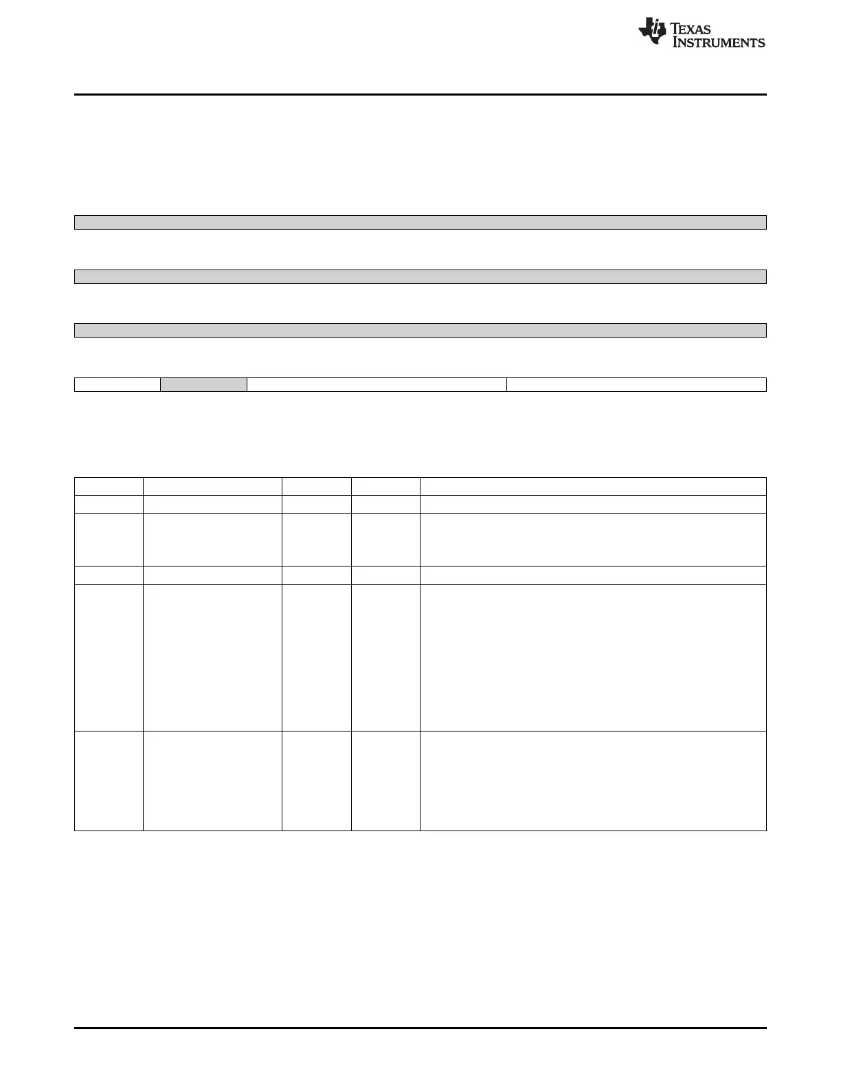
8.1.12.5.1 CM_CLKOUT_CTRL Register (offset = 0h) [reset = 0h]
CM_CLKOUT_CTRL is shown in Figure 8-154 and described in Table 8-165.
This register provides the control over CLKOUT2 output
Figure 8-154. CM_CLKOUT_CTRL Register
31 30 29 28 27 26 25 24
Reserved
R-0h
23 22 21 20 19 18 17 16
Reserved
R-0h
15 14 13 12 11 10 9 8
Reserved
R-0h
7 6 5 4 3 2 1 0
CLKOUT2EN Reserved CLKOUT2DIV CLKOUT2SOURCE
R/W-0h R-0h R/W-0h R/W-0h
LEGEND: R/W = Read/Write; R = Read only; W1toCl = Write 1 to clear bit; -n = value after reset
Table 8-165. CM_CLKOUT_CTRL Register Field Descriptions
Bit Field Type Reset Description
31-8 Reserved R 0h
7 CLKOUT2EN R/W 0h
This bit controls the external clock activity
0x0 = DIS : SYS_CLKOUT2 is disabled
0x1 = EN : SYS_CLKOUT2 is enabled
6 Reserved R 0h
5-3 CLKOUT2DIV R/W 0h
THis field controls the external clock divison factor
0x0 = DIV1 : SYS_CLKOUT2/1
0x1 = DIV2 : SYS_CLKOUT2/2
0x2 = DIV3 : SYS_CLKOUT2/3
0x3 = DIV4 : SYS_CLKOUT2/4
0x4 = DIV5 : SYS_CLKOUT2/5
0x5 = DIV6 : SYS_CLKOUT2/6
0x6 = DIV7 : SYS_CLKOUT2/7
0x7 = Reserved
2-0 CLKOUT2SOURCE R/W 0h
This field selects the external output clock source
0x0 = SEL0 : Select 32KHz Oscillator O/P
0x1 = SEL1 : Select L3 Clock
0x2 = SEL2 : Select DDR PHY Clock
0x3 = SEL4 : Select 192Mhz clock from PER PLL
0x4 = SEL5 : Select LCD Pixel Clock
8.1.12.6 CM_RTC Registers
Table 8-166 lists the memory-mapped registers for the CM_RTC. All register offset addresses not listed in
Table 8-166 should be considered as reserved locations and the register contents should not be modified.
692
Power, Reset, and Clock Management (PRCM) SPRUH73H–October 2011–Revised April 2013
Submit Documentation Feedback
Copyright © 2011–2013, Texas Instruments Incorporated

 Loading...


