EMIF
www.ti.com
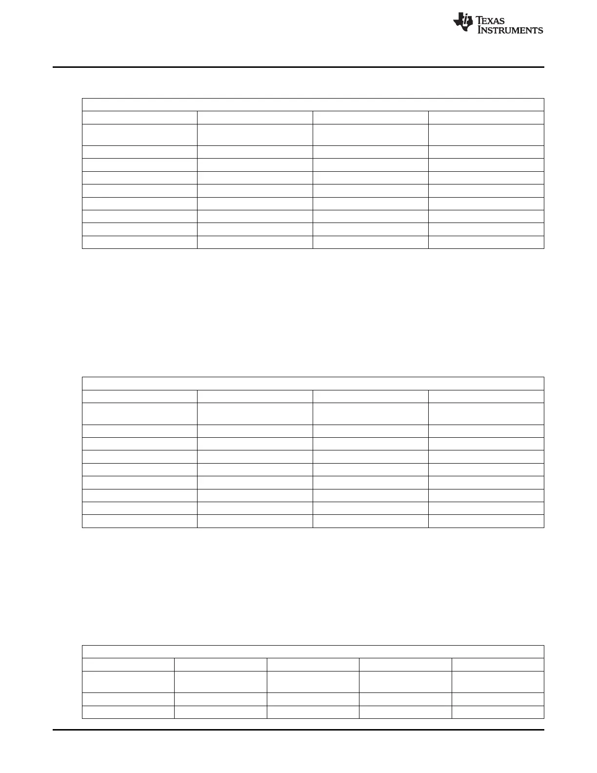
Table 7-103. OCP Address to DDR2/3/mDDR Address Mapping for REG_IBANK_POS=3 and
REG_EBANK_POS=0
Logical Address
Bank Address Row Address Chip Select Column Address
# of bits defined by IBANK of # of bits defined by RSIZE of # of bits defined by EBANK of # of bits defined by PAGESIZE
SDRCR SDRCR SDRCR of SDRCR
IBANK=0 => 0 bits RSIZE=0 => 9 bits EBANK=0 => 0 bits PAGESIZE=0 => 8 bits
IBANK=1 => 1 bit RSIZE=1 => 10 bits EBANK=1 => 1 bit PAGESIZE=1 => 9 bits
IBANK=2 => 2 bits RSIZE=2 => 11 bits PAGESIZE=2 => 10 bits
IBANK=3 => 3 bits RSIZE=3 => 12 bits PAGESIZE=3 => 11 bits
RSIZE=4 => 13 bits
RSIZE=5 => 14 bits
RSIZE=6 => 15 bits
RSIZE=7 => 16 bits
7.3.3.4.5 Address Mapping when REG_IBANK_POS = 0 and REG_EBANK_POS = 1
For REG_IBANK_POS = 0 and REG_EBANK_POS = 1, the DDR2/3/mDDR memory controller interleaves
among all the banks within a device (per chip select). However, the DDR2/3/mDDR memory controller
cannot interleave banks between the two chip selects. Thus, the DDR2/3/mDDR memory controller can
keep a maximum of 16 banks (8 internal banks across 2 chip selects) open at a time, but can only
interleave among 8 of them.
Table 7-104. OCP Address to DDR2/3/mDDR Address Mapping for REG_IBANK_POS=0 and
REG_EBANK_POS=1
Logical Address
Chip Select Row Address Bank Address Column Address
# of bits defined by EBANK of # of bits defined by RSIZE of # of bits defined by IBANK of # of bits defined by PAGESIZE
SDRCR SDRCR SDRCR of SDRCR
EBANK=0 => 0 bits RSIZE=0 => 9 bits IBANK=0 => 0 bits PAGESIZE=0 => 8 bits
EBANK=1 => 1 bit RSIZE=1 => 10 bits IBANK=1 => 1 bit PAGESIZE=1 => 9 bits
RSIZE=2 => 11 bits IBANK=2 => 2 bits PAGESIZE=2 => 10 bits
RSIZE=3 => 12 bits IBANK=3 => 3 bits PAGESIZE=3 => 11 bits
RSIZE=4 => 13 bits
RSIZE=5 => 14 bits
RSIZE=6 => 15 bits
RSIZE=7 => 16 bits
7.3.3.4.6 Address Mapping when REG_IBANK_POS = 1 and REG_EBANK_POS = 1
For REG_IBANK_POS = 1 and REG_EBANK_POS = 1, the interleaving of banks within a device (per chip
select) is limited to 4 banks. Also, the DDR2/3/mDDR memory controller cannot interleave banks between
the two chip selects. Thus, the DDR2/3/mDDR memory controller can keep a maximum of 16 banks (8
internal banks across 2 chip selects) open at a time, but can only interleave among four of them.
Table 7-105. OCP Address to DDR2/3/mDDR Address Mapping for REG_IBANK_POS=1 and
REG_EBANK_POS = 1
Logical Address
Chip Select Bank Address[2] Row Address Bank Address[1:0] Column Address
# of bits defined by # of bits defined by # of bits defined by # of bits defined by # of bits defined by
EBANK of SDRCR IBANK of SDRCR RSIZE of SDRCR IBANK of SDRCR PAGESIZE of SDRCR
EBANK=0 => 0 bits IBANK=0 => 0 bits RSIZE=0 => 9 bits IBANK=0 => 0 bits PAGESIZE=0 => 8 bits
EBANK=1 => 1 bit IBANK=1 => 0 bits RSIZE=1 => 10 bits IBANK=1 => 1 bit PAGESIZE=1 => 9 bits
412
Memory Subsystem SPRUH73H–October 2011–Revised April 2013
Submit Documentation Feedback
Copyright © 2011–2013, Texas Instruments Incorporated

 Loading...


