ECC-A[0]
...
ECC-A[25]
0
2
27
28
ECC-B[0]
...
ECC-B[25]
ECC-C[0]
...
ECC-C[25]
ECC-D[0]
...
ECC-D[25]
53
54
79
80
105
ECC-A[1] ECC-A[0]
...
0
1
...
ECC-A[24]ECC-A[25]
ECC-B[0]ECC-B[1]
......
ECC-B[24]ECC-B[25]
13
14
26
byte x8 word x16
MSB LSB
ECC-H[0]ECC-H[1]
......
ECC-H[24]ECC-H[25]
92
104
ECC-E[0]
...
ECC-E[25]
106
131
132
ECC-F[0]
...
ECC-F[25]
ECC-G[0]
...
ECC-G[25]
ECC-H[0]
...
ECC-H[25]
157
158
183
184
209
ECC-C[0]ECC-C[1]
......
ECC-C[24]ECC-C[25]
27
39
1
Functional Description
www.ti.com
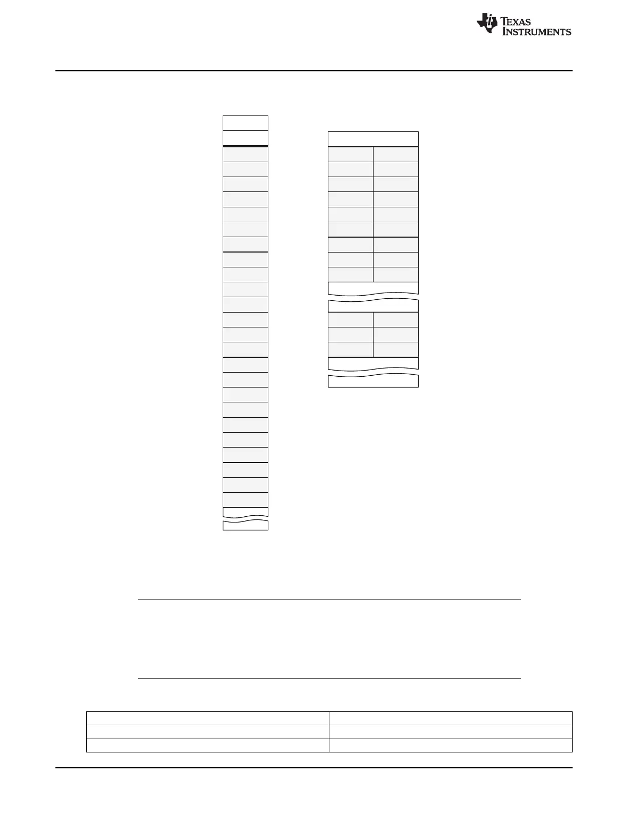
Figure 26-16. ECC Data Mapping for 4 KB Page and 16b BCH Encoding
26.1.7.4.2.2 Pins Used
The list of device pins that are configured by the ROM in the case of NAND boot mode are as follows.
Please note that all the pins might not be driven at boot time.
NOTE: Caution must be taken when using an 8-bit NAND. The ROM initially configures all address
and data signals (AD0-AD15) the GPMC uses when attempting to read configuration values
from the NAND. If you use an 8-bit NAND, and connect AD15-AD8 to other functions
(GPIOs, for example), there may be contention on these signals during the boot phase.
AD15-AD8 are configured as outputs and will be driven by the ROM if NAND boot is
selected. Ensure external circuits will not be in contention with these driven outputs.
Table 26-19. Pins Used for NAND Boot
Signal name Pin Used in Device
CS0 GPMC_CSN0
ADVN_ALE GPMC_ADVN_ALE
4128
Initialization SPRUH73H–October 2011–Revised April 2013
Submit Documentation Feedback
Copyright © 2011–2013, Texas Instruments Incorporated

 Loading...


