GPMC_FCLK
GPMC_CLK
nBE1/nBE0
nCS
nADV
nOE
nWE
DIR
WAIT
Valid Address
Valid Address
D 0
D 3
D 4
D 5
D 6
D 7
OUT
CSONTIME
CSWROFFTIME
ADVONTIME
ADVWROFFTIME
WRDATAONADMUXBUS
WEONTIME
WEOFFTIME
OEAADMUXOFFTIME
CLKACTIVATIONTIME
WRACCESSTIME
WRCYCLETIME0
A[27:17]
A[16:1]/D[15:0]
D 1
D 2
D 7
PAGEBURSTACCESSTIME
PAGEBURSTACCESSTIME
PAGEBURSTACCESSTIME
WRCYCLETIME1
OEAADMUXOFFTIME
OEAADMUXONTIME
OEAADMUXONTIME
www.ti.com
GPMC
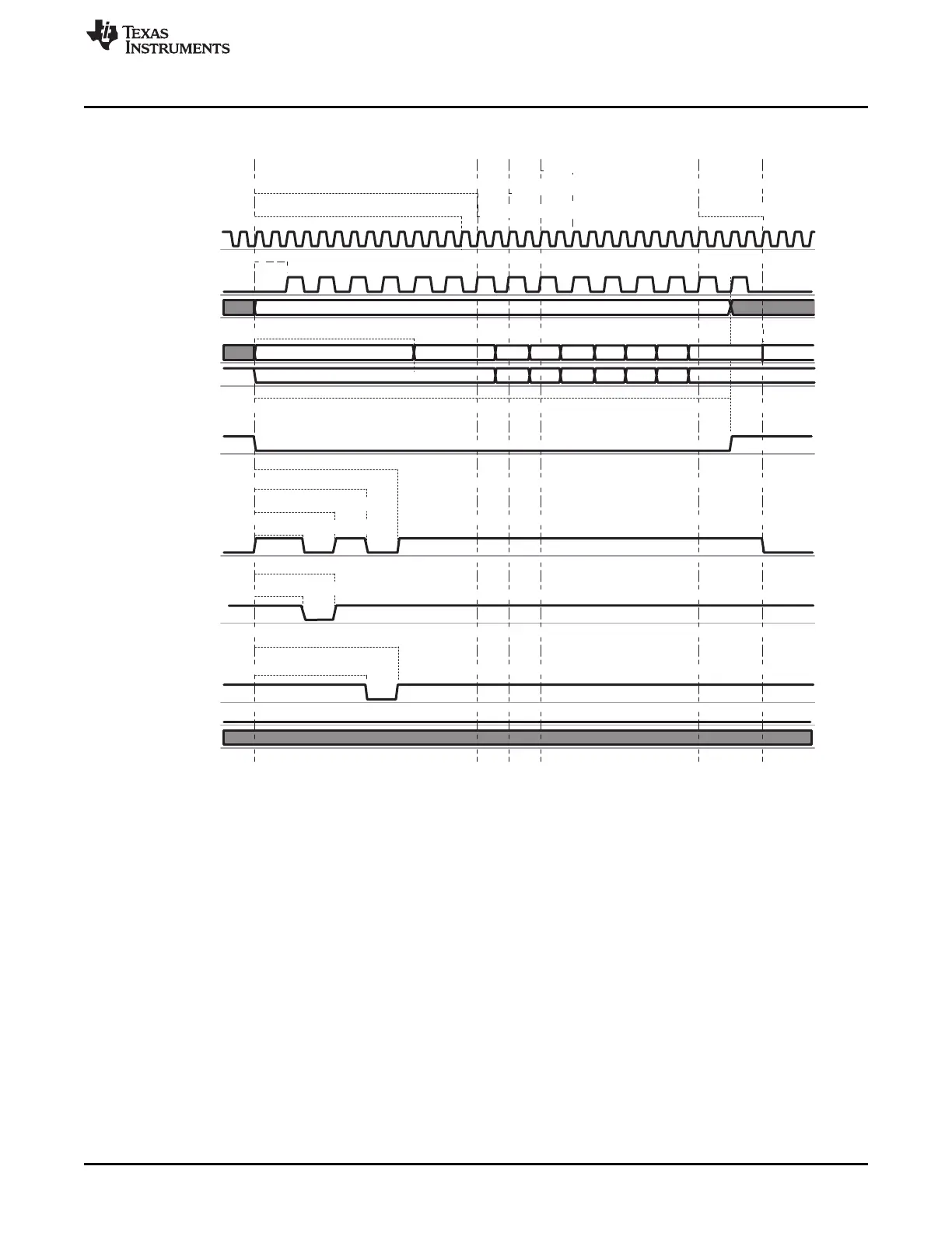
Figure 7-23. Synchronous Multiple Write (Burst Write) in Address/Address/Data-Multiplexed Mode
The first data of the burst is driven on the A/D bus at GPMC_CONFIG6_i[19:16]
WRDATAONADMUXBUS.
When WRACCESSTIME completes, control-signal timings are frozen during the multiple data
transactions, corresponding to the GPMC_CONFIG5_i[27-24] PAGEBURSTACCESSTIME multiplied by
the number of remaining data transactions.
When the GPMC generates a read access to an address/data-multiplexed device, it drives the address
bus until OEn assertion time. For details, see Section 7.1.3.3.8.2.3.
• Chip-select signal CSn
– CSn assertion time is controlled by the GPMC_CONFIG2_i[3-0] CSONTIME field and ensures
address setup time to CSn assertion.
– CSn deassertion time controlled by the GPMC_CONFIG2_i[20-16] CSWROFFTIME field and
ensures address hold time to CSn deassertion.
• Address valid signal ADVn
– ADVn assertion time is controlled by the GPMC_CONFIG3_i[3-0] ADVONTIME field.
– ADVn deassertion time is controlled by the GPMC_CONFIG3_i[20-16] ADVWROFFTIME field.
295
SPRUH73H–October 2011–Revised April 2013 Memory Subsystem
Submit Documentation Feedback
Copyright © 2011–2013, Texas Instruments Incorporated
 Loading...


