GPMC_FCLK
GPMC_CLK
WAIT
D 0
CSONTIME
ADVONTIME
ADVRDOFFTIME
OEONTIME
OEOFFTIME
CLKACTIVATIONTIME
CSRDOFFTIME
RDCYCLETIME
RDACCESSTIME
nBE1/nBE0
nCS
nADV
nOE
DIR OUT IN OUT
Valid Address
Valid Address
A[27:17]
A[16:1]/D[15:0]
WRDATAONADMUXBUS
www.ti.com
GPMC
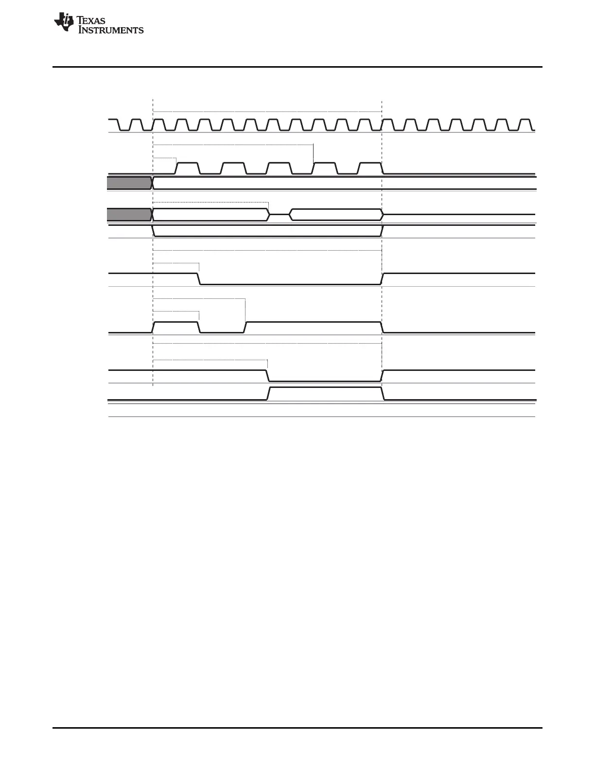
Figure 7-18. Synchronous Single Read (GPMCFCLKDIVIDER = 1)
See Section 7.1.3.9.1 for formulas to calculate timing parameters.
Table 7-41 lists the timing bit fields to set up in order to configure the GPMC in asynchronous single read
mode.
When the GPMC generates a read access to an address/data-multiplexed device, it drives the address
bus until OEn assertion time. For details, see Section 7.1.3.3.8.2.3.
• Chip-select signal CSn
– CSn assertion time is controlled by the GPMC_CONFIG2_i[3-0] CSONTIME field and ensures
address setup time to CSn assertion.
– CSn deassertion time is controlled by the GPMC_CONFIG2_i[12-8] CSRDOFFTIME field and
ensures address hold time to CSn deassertion.
• Address valid signal ADVn
– ADVn assertion time is controlled by the GPMC_CONFIG3_i[3-0] ADVONTIME field.
– ADVn deassertion time is controlled by the GPMC_CONFIG3_i[12-8] ADVRDOFFTIME field.
• Output enable signal OEn
– OEn assertion indicates a read cycle.
– OEn assertion time is controlled by the GPMC_CONFIG4_i[3-0] OEONTIME field.
– OEn deassertion time is controlled by the GPMC_CONFIG4_i[12-8] OEOFFTIME field.
• Initial latency for the first read data is controlled by GPMC_CONFIG5_i[20-16] RDACCESSTIME or by
monitoring the WAIT signal.
• Total access time (GPMC_CONFIG5_i[4-0] RDCYCLETIME) corresponds to RDACCESSTIME plus
the address hold time from CSn deassertion, plus time from RDACCESSTIME to CSRDOFFTIME.
289
SPRUH73H–October 2011–Revised April 2013 Memory Subsystem
Submit Documentation Feedback
Copyright © 2011–2013, Texas Instruments Incorporated
 Loading...


