GPMC_FCLK
GPMC_CLK
WAIT
Valid address 0 Valid address 1
Data 0
Valid address 0 Valid address 1
Data 1
Data 1
CSONTIME CSONTIME
CSRDOFFTIME CSRDOFFTIME
ADVONTIME ADVONTIME
ADVRDOFFTIME ADVRDOFFTIME
OEONTIME OEONTIME
OEOFFTIME OEOFFTIME
RDCYCLETIME RDCYCLETIME
CYCLE2CYCLEDELAY
nBE1/nBE0
nCS
nADV
nOE
DIR OUT OUT OUTIN IN
A[27:17]
A[16:1]/D[15:0]
GPMC
www.ti.com
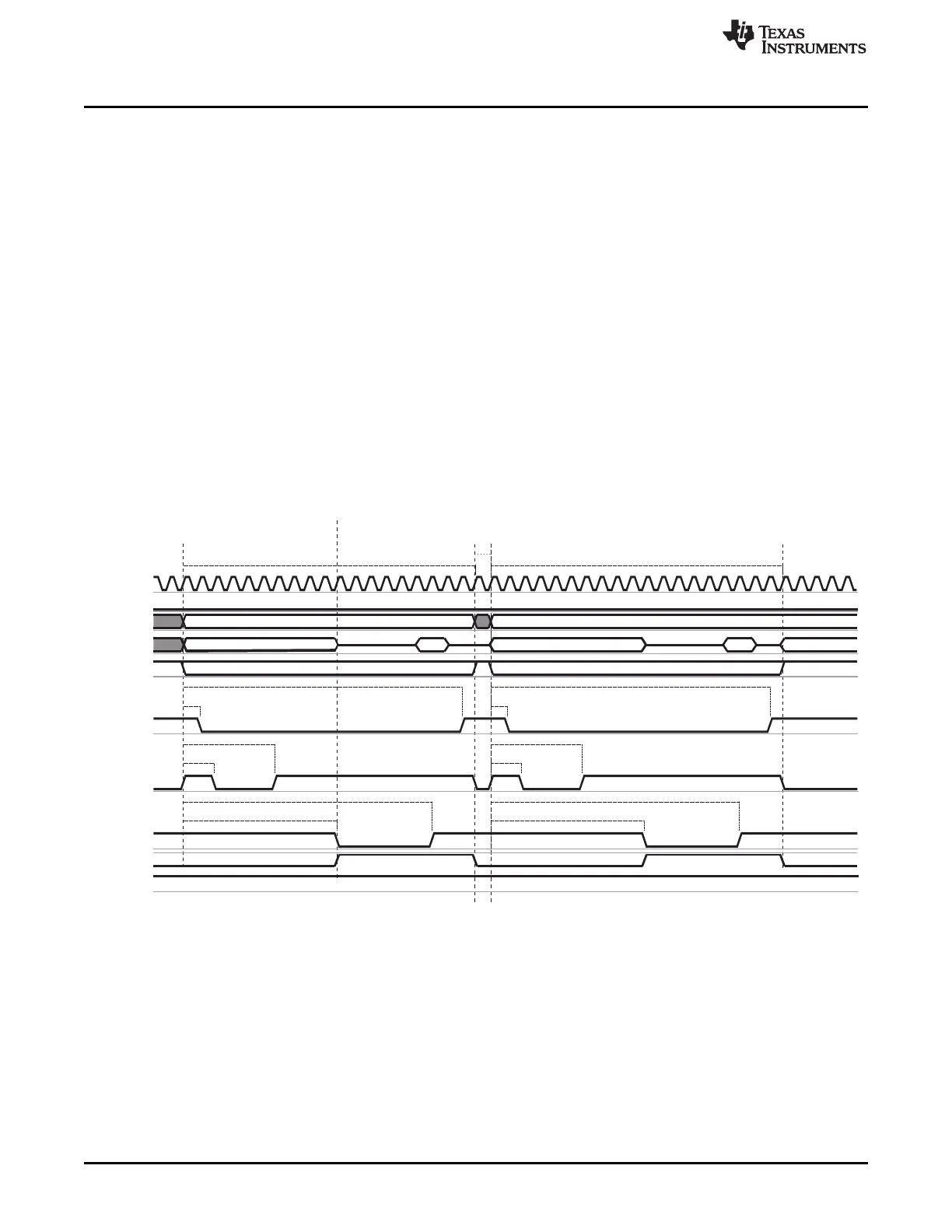
• Output enable signal OEn
– OEn assertion indicates a read cycle.
– OEn assertion time is controlled by the GPMC_CONFIG4_i[[3-0] OEONTIME field.
– OEn deassertion time is controlled by the GPMC_CONFIG4_i[[12-8] OEOFFTIME field.
• Read data is latched when RDACCESSTIME completes. Access time is defined in the
GPMC_CONFIG5_i[20-16] RDACCESSTIME field.
• Direction signal DIR: DIR goes from OUT to IN at the same time that OEn is asserted.
• The end of the access is defined by the GPMC_CONFIG5_i[4-0] RDCYCLETIME parameter.
In the GPMC, when a 16-bit wide device is attached to the controller, a 32-bit word write access is split
into two 16-bit word write accesses. For more information about GPMC access size and type adaptation,
see Section 7.1.3.3.10.5. Between two successive accesses, if a OEn pulse is needed:
• The GPMC_CONFIG6_i[[11-8] CYCLE2CYCLEDELAY field can be programmed with
GPMC_CONFIG6_i[[7] CYCLE2CYCLESAMECSEN enabled.
• The CSWROFFTIME and CSONTIME parameters also allow a chip-select pulse, but this affects all
other types of access.
Figure 7-13 shows two asynchronous single-read accesses on an address/data-multiplexed devices.
Figure 7-13. Two Asynchronous Single Read Accesses on an Address/Data Multiplexed Device
(32-Bit Read Split Into 2 × 16-Bit Read)
282
Memory Subsystem SPRUH73H–October 2011–Revised April 2013
Submit Documentation Feedback
Copyright © 2011–2013, Texas Instruments Incorporated

 Loading...


